News Posts matching #Die Shrink

Return to Keyword Browsing

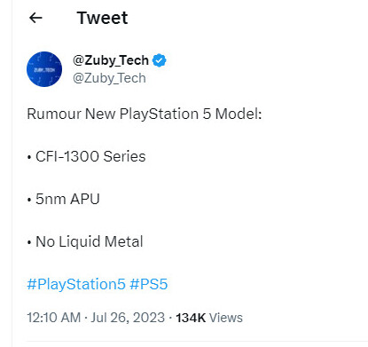
Leaker Claims No Liquid Metal Cooling for PlayStation 5 Refresh

PlayStation 5-related rumors have been flowing over the past week—Zuby_Tech was reportedly the main source responsible for leaking out Project Q footage, but the tipster has turned to his attention to an alleged new version of the host system. Yesterday's tweet makes reference to a refreshed PlayStation 5 model—the "CFI-1300 series"—with a revised 5 nm APU. The late-2020 launch model (CFI-1200) sported a 7 nm chipset, while 2022's die shrink granted the CFI-1202 series with a 6 nm SoC.

The tipster thinks that Sony will be dropping the PS5's liquid metal cooling system for its next iteration, thanks to a central 5 nm part offering greater efficiency and reduced thermal output. Previous reports have predicted that this refreshed "modular model" is marked for a late 2023 release window. Sony has been running a summer price reduction campaign—could this marketing incentive be clearing the way—i.e selling off older stock—in anticipation of the refreshed model's arrival? "CFI-1300" should not be confused with the heavily rumored PlayStation 5 Pro variant—Insider Gaming's Tom Henderson has reiterated multiple times that this major hardware upgrade is still a long way off from launching.

NVIDIA plans 45 nm chip in 2008

NVIDIA is working on its 45 nanometre part. This year, the company plans to migrate to 65 nanometre as much as possible, but by the end of 2008 it should have 45 nanometre parts ready.

The company first has to shrink its 65 nanometre chips to 55 nanometre as this is the optical shrink and later it will go for 45 nanometre. Intel announced it will go 45 nanometre in late Q4 07 / early Q1 2008, AMD said that for its CPUs it will be able to do it by the mid of 2008.

The good thing about 45 nanometre chips is that on 15x15 square millimetres die you can put 1,350 millions of transistors or roughly twice as much as you can do with 65 nanometre.

After that the next big step is 32 nanometre scheduled for 2010.

Intel Penryn details

Penryn is Intels next generation of the Core 2 Duo with 'Conroe'-core. Based on a 45nm process and an improved High-k dielectric together with metal gates the Penryn features the SSE4 instruction set (aka Nehalem New Instructions, NNI), and a 6MB/12MB L2-cache (Core 2 Duo/Core 2 Quad). Power consumption will roughly be the same, 65W TDP for the Duo and 105W for the Quad. The working frequencies will be higher than 3GHz for the top models resulting in around 20% more performance when playing games. Video-trancoding that utilizes the new SSE4 instructions will be around 40% faster Intel says.
The mobile Penryn features an additional 'deep power down'-state where both caches will be deactivated, the core-frequency and -voltage are lowered by a significant amount. Furthermore the chip is able to change both core's frequencies and voltages indepentently from one another. Let's say you are using a single threaded application for a while the second core won't have much to do it will power itself down whereas the other core could power it up to improve the performance.
In late 2008 Intel plans to release the Nehalem architecture which comes with an integrated memory controller. By then the front side bus days will be over, a serial Hypertransport-like interface called 'CSI' (Common System Interface) will replace it.

Update: AnandTech covers the story as well with a whole article dedicated to the Penryn and Nehalem.

R600 will come in 65nm

Everyone who could attend the HIS press dinner yesterday in the evening was surely disappointed afterwards. HIS had to inform the invited journalists that they won't see the R600 at HIS' booth - not even behind closed doors! - I guess GeCube won't show the chip neither, though they promised to do so! - ATI/AMD then let the press people know they will set up a special Tech-Day until the 31st of March and disclosed some new information. The R600 will be produced in 65nm by TSMC and not using the 80nm process because of difficulties (low yield and high leakage current). Daniel Wenzel from the German K-Hardware adds rumours have it AMD/ATI still got issues with the 512 bit memory subsystem. I nearly forgot to add the newly planned release date: Six weeks from now which reads begin of May.

PS3 Cell processor now manufactured in 65nm

According to DailyTech IBM is from now on producing the Playstation 3 powering 'Cell' processor in it's Fab in East Fishkill (N.Y.) using a 65nm process. Interestingly this particular chip factory is the same where the microprocessors that power Nintendo's Wii come from.
The shrink to 65nm will help reducing the cost (Sony is still losing money when selling it's console) and the power consumption of the system as well.

Sony 65nm SOI Cell Broadband Engine Details

ISSCC (International Solid-State Circuits Conference) seems to be packed with interesting stuff this year. Earlier today, we reported how Samsung demonstrated 4 GHz GDDR4 memory modules at the conference, and now, VR-Zone reports that the Cell Broadband Engine is in for a die-shrink. The 'new' 65nm chip will replace the current 90nm units that can be found in PS3s. It is smaller as compared to the 90nm version, thus it is cheaper to produce and emits less heat. Also, the SRAM on the 65nm Cell B.E is improved. Sony engineers managed to run the 65nm Cell B.E. chip at 6GHz with just 1.3V. Sony is expected to continue using Cell B.E. architecture into their next generation PlayStation 4 and there is a possibility that IBM's eDRAM technology will be employed.

G90 will be a 65nm G80 with 512-bit GDDR4

Or at least, that's the current rumor. While we debate the current R600 rumors, The Inquirer is claiming that their "senior industry sources" have let loose the first G90 details rumors. The G90 will undertake the monumental task of putting the G80 through a die shrink. If all goes well, this will allow for very high clocks, much lower power consumption, and a lower production cost. NVIDIA also hopes to get hold of some GDDR4 for the G90, and will put it on a 512-bit bus.

NVIDIA to shrink G72 to make G78

The G78 will be a 65nm version of the G72. Instead of being themed for basic video or games, it is themed around a low-power, Vista-ready solution. This G78 will only be expected to run Aero glass, an occasional DVD, and flash-based games. It will be produced with the G84 series, have a 64 bit memory interface, and will cost $60 or less.

Intel plans to enter graphics field with multi-core 32nm GPU

As you probably know, Intel is working on their own graphics card. Most people scoff at this idea, considering that Intel was rumored to buy NVIDIA so that they could have graphics cards. However, in a few years (late 2008/2009), Intel is planning on becoming a serious threat to the market dominance owned by NVIDIA and ATI. Intel is claiming that by late 2008 they will have at least sampled a card with multiple cores (up to sixteen) on one die. They also claim they will be able to do this on a 32nm architecture. This 16 core, 32nm GPU is estimated to run sixteen times faster than the 8800GTX.

45nm Opterons in 2008

AMD has released some information about its Shanghai processors - the next generation of server CPUs after the Barcelona cores. The Shanghai processors will be the company's first 45nm chips, which should bring power consumption and heat benefits over 90nm and 65nm equivilents. They will also have 6MB of L3 cache and use the socket 1207 interface, so should be able to work with current Socket F motherboards providing BIOS updates are released. The Shanghai is likely to compete with Intel's 45nm offering, known as Penryn.

Intel shows off 45nm Penryn

The Intel Core 2 Duo series is about to embark on a die shrink, from 65nm to 45nm. The new Core 2 Duo's, codenamed "Penryn", will have a slew of new features. The Penryn's will support a new set of SSE instructions, have higher clock speeds while maintaining the same power draw, and have a larger L2 Cache. The dual core Penryn will have 410 million transistors, and the quad core Penryn will have 820 million. All of the Penryn's will be on a 300mm package. Like with the current generation quad core offerings, the quad core Penryn's will have two dual core processors on one package. The Penryn series will have the same power requirements as the Conroe, which translates to 35W laptop chips, 65W dual-core desktop chips, and 80W quad-core desktop chips. Intel has successfully tested the Penryn's on several operating systems for stability, and we should see something commercially available around Q2 2007.

NVIDIA G81 rumored to be on a 65 nanometer process

In the recent DX10 graphics card war, NVIDIA has gotten a very long headstart. Not only has NVIDIA had enough time to develop watered-down versions of their G80 for selling as entry-level and midrange cards, but they've also had time to develop "G81". The current specs of what G81 could be are currently unknown, but it does have one major goal- a shrink to a 65 nanometer process. This would represent a gigantic step in the graphics card world, as GPU makers have barely made the step to 80nm GPU's recently. It would also, like most die shrinks, decrease power input and heat output.

AMD to Launch New 65nm CPUs

AMD will soon be ready to ship another series of single-core 65nm Athlon 64 processors, according to HKEPC. The new models help in lowering the cost as well as the power consumption from 62W to 45W (27.4%). The two desktop processors to be launched in Mid-Jan, codenamed Lime, include Athlon 64 3500+ and Athlon 64 3800+. Basically, the 65nm models are the same as the 90nm edition. They are clocked at 2.2GHz and 2.4GHz respectively, and have 512KB of L2 cache. In addition 10 more 65nm models will be released in Q2 2007. The upcoming models include three new dual-core Athlon 64 X2 35W TDP processors codenamed Brisbane and one single core Athlon 64 4000+(2.6GHz 45W TDP). For the entry level AMD also plans to release four 65nm Sempron models with 35W TDP, codenamed Sparta. Please click here to learn more.

SAMSUNG Samples First 50nm 16Gb NAND Flash

Samsung Electronics Co., Ltd., the world leader in advanced semiconductor technology solutions, announced that it is now sampling its 16-gigabit(Gb) NAND flash memory with customers - the first NAND flash using 50 nanometer(nm) process technology. The first samples of this high density NAND flash memory have a multi-level cell(MLC) design with a 4Kbyte(KB) page size to enhance both its read and write features. The new 4KB page function improves the conventional 2KB paging system for MLC NAND flash to double the read speed, while increasing write performance 150%.

65nm Xbox 360 CPUs Delayed Until mid-2007

According to industry sources, plans to produce CPUs for the Microsoft Xbox 360 game console on 65nm at Chartered Semiconductor Manufacturing will be pushed back until the middle of 2007. In April 2006, Chartered announced that it had signed an agreement with Microsoft to manufacture CPUs for the Xbox 360 console on 65nm Silicon-on-Insulator (SOI) technology starting in the first quarter of 2007. Chartered is already a major foundry partner for producing Microsoft's Xbox 360 CPUs on 90nm technology. Both companies declined to comment on the news.

Elpida Memory Begins World's First Mass Production of 70nm DRAM


Elpida Memory, Inc. (Elpida), Japan's leading global supplier of Dynamic Random Access Memory (DRAM), announced that it has begun mass production of the DRAM industry's first 1-Gigabit and 512-Megabit DDR2 SDRAMs using 70-nanometer process technology. Manufacturing will be done at its main fab facility, Hiroshima Elpida Memory, Inc. Elpida, a leading provider of advanced DRAM products, is currently realizing high yields and productivity from its 90nm process technology used in mass production. The technology that has made those achievements possible has been applied to the development of the more advanced 70nm process technology.

Sparkle produces first video card with 80nm NVIDIA GPU

Sparkle has officially beaten all the other NVIDIA manufacturers to making a card based on an 80nm GPU. The first 80nm GPU from NVIDIA is a blue 7600GT, based off of the G73 (there is no information on what NVIDIA calls the 80nm version of the G73). The card comes clocked at 650MHz, a full 90MHz faster then 7600GT stock specifications. The memory and memory controller is still the same. The memory is clocked at 1600MHz DDR, and is only 128 bit. The card comes with 12 ROP's, 256MB of memory, and a PCI Express x16 interface. The card should be available in 2007, and offers significant performance benefits when compared to the 90nm version of the same card (roughly 500 points in 3Dmark06).

Hynix Develops 60nm 1Gb DDR2 800MHz Modules

Hynix Semiconductor has developed the world's first 800 MHz memory module using 60nm 1GB DDR2 DRAM. The chipmaker received approval for its 60nm DRAM chip from Intel in October and has now developed the 60nm DDR2 memory module this time, passing Intel's Advanced Validation Lab (AVL) test. The new memory chip comes in two types: one with a speed of 800 MHz and the other with a speed of 667 MHz. It also helps hike productivity by a whopping 50 percent, the chipmaker says. In addition, such cutting edge technologies as a "three-dimensional" transistor and three-layered metal allocation boost storage capacity and processing speeds. Hynix is expected to start mass production in the first half of 2007 and use the new memory chip in making high density DRAM components and high performance products such as graphic and mobile DRAMs.

AMD 65nm products soon

This year, Intel boasted at IDF about being the only company shipping 65nm chips. This is about to change.

The Inquirer reports that system integrators already have their hands on AMD's 65nm X2 CPUs. They have been shipping for 2 weeks already. The CPUs will be available to the public early 2007, yet they will be nothing more than a re-designed 90nm part.

If you're lucky, you could find one of these in an assembled HP or Dell AMD machine this year.

Below is a picture of AMD's 65nm X2 CPU:

AMD and IBM Detail Early 45nm Results

At the International Electron Device Meeting (IEDM) today, IBM and AMD presented papers describing the use of immersion lithography, ultra-low-K interconnect dielectrics, and multiple enhanced transistor strain techniques for application to the 45nm microprocessor process generation. AMD and IBM expect the first 45nm products using immersion lithography and ultra-low-K interconnect dielectrics to be available in mid-2008.

AMD drives next generation of energy-efficient computing with 65nm technology transition

SUNNYVALE, CALIF. -- December 5, 2006 --Launching the next generation of energy-efficient computing, AMD (NYSE: AMD) today announced the transition to 65nm process technology, beginning with the immediate availability of energy-efficient AMD Athlon 64 X2 dual-core desktop processors. The move to 65nm process technology enables AMD to produce more processors on a 300mm wafer, for increased production capacity, while continuing to aggressively scale performance and reduce power consumption. AMD processors built with 65nm line-widths are designed to deliver exceptional performance when running multiple applications, as well as enable small form factor PCs that complement both home and office environments. By mid-2007, AMD expects to be fully converted to 65nm production at Fab 36. With the rapid conversion to 65nm process technology, AMD is scaling capacity intelligently to meet growing demand worldwide for x86 processors.
Return to Keyword Browsing
May 4th, 2024 00:18 EDT change timezone

New Forum Posts

Popular Reviews

Controversial News Posts