News Posts matching #IGP

Return to Keyword Browsing

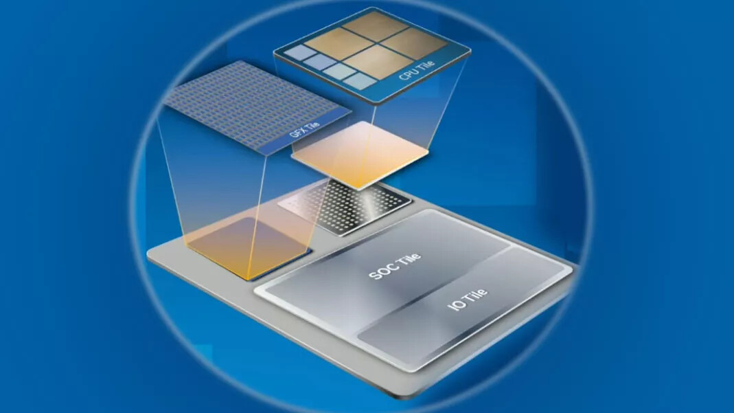
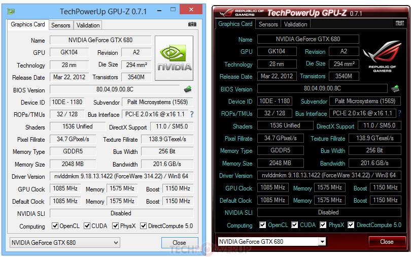
Intel 14th Gen "Meteor Lake" APUs Reportedly Feature Ray Tracing, May Lack XeSS

Intel's future Meteor Lake APUs seem to be playing catch-up to AMD's integrated graphics in more ways than one. Twitter user Coelacanth's Dream has dug up information that indicates Intel's commitment to bring ray tracing support to even its IGP (Integrated Graphics Processing) tiles. According to bits and pieces from Intel Graphics Compiler (IGC) code patches, it seems to be confirmed that ray tracing support is indeed coming to the TSMC-made, 3 nm GPU tiles in Meteor Lake. The kicker here is the presence of flags that detect whether the iGPU is of the "iGFX_meteorlake" type - if so, IGC sets ray tracing support to enabled.

Puzzlingly, Intel's upscaling technology, Xe SuperSampling (XeSS) could be out of the picture - at least for now. It seems that IGC patches for the upcoming APU family still don't allow for DPAS (Dot Product Accumulate Systolic) instructions - instructions that rely on XMX (Intel Xe Matrix Extensions), the AI engines responsible for executing 128 FP16/BF16, 256 INT8, or 512 INT4/INT2 operations per clock. These low-precision operations are the soul of algorithmic supersampling technologies such as XeSS.

Benchmarks Surface on Intel's Next-Gen Comet Lake-S 10-Core, 6-Core CPUs

Benchmarks have been uploaded to popular benchmarking utility Geekbench's servers, and they seemingly allow us to look into Intel's next-gen Comet Lake-S processors. The results, which have likely been taken from pre-release hardware (which means benchmarks and even proper identification of features on the CPUs shouldn't be taken as guarantees), help paint a picture on Intel's next release all the same.

Processor information for the 10-core, 20-thread CPU gives us a 1.51 GHz base clock and 3.19 GHz boost, with the chip featuring 32 Kb each for L1 instruction and L1 data caches (x10 cores, 640 KB total) 256 KB L2 cache (x10 cores, for a total of 2.5 MB) and 20 MB L3 cache. The six-core part, on the other hand, is reported as featuring a 1.99 GHz base clock and 2.89 GHz boost clock, 384 KB total L1 instruction and data caches (32 KB x 6 cores), 256 KB L2 cache (x6 cores, for a total of 1.5 MB) and 12 MB L3 cache. This means each core is in Comet Lake-S is paired with 2 MB of L3 cache, which is being cut-down alongside cores. Like almost all other Intel desktop CPU releases, these CPU cores will be paired with an IGP in the form of Intel UHD Graphics 630, which features up to 24 Execution Units (EUs). With Intel's 10-core CPU being expected to be the cream of the crop on the company's mainstream CPU lineup come Comet Lake-S, comparisons to AMD's own core density are moot, in that there is no real competition available, should that top core count actually materialize.

NVIDIA Adds New Options to Its MX200 Mobile Graphics Solutions - MX250 and MX230

NVIDIA has added new SKUs to its low power mobility graphics lineup. the MX230 and MX250 come in to replace The GeForce MX130 and MX150, but... there's really not that much of a performance improvement to justify the increase in the series' tier. Both solutions are based on Pascal, so there are no Turing performance uplifts at the execution level.

NVIDIA hasn't disclosed any CUDA core counts or other specifics on these chips; we only know that they are paired with GDDR 5 memory and feature Boost functionality for increased performance in particular scenarios. The strange thing is that NVIDIA's own performance scores compare their MX 130, MX150, and now MX230 and MX250 to Intel's UHD620 IGP part... and while the old MX150 was reported by NVIDIA as offering an up to 4x performance uplift compared to that Intel part, the new MX250 now claims an improvement of 3.5x the performance. Whether this is because of new testing methodology, or some other reason, only NVIDIA knows.

Intel's IGP-less i9-9900KF, i7-9700KF CPUs First Listings Appear Above MSRP Pricing

Intel will be relasing IPG-less versions of their most popular desktop processors soon, if some retailers' listings of the CPUs are anything to go by. The i9-9900KF and i7-9700KF CPUs will bring about Intel's best-performing architecture to date in an integrated GPU-less package, which will allow the company to bring prices down for the end user. Of course, this has all the hallmarks of a bid for a more competitive positioning of its products against AMD's upcoming Zen 2 products, whilst simultaneously (and likely) increasing profit on every processor sold (we'd expect the savings passed on to the customer to be inferior to Intel's saved costs at the foundry level).

The i9-9900KF has been found online for $582.50, more than $50 above the i9-9900K's $530 street pricing, while the 9600KF is listed at $308.75, more than $60 over the street pricing of Intel's i7-9600K. Remember that these prices are gouged on account of limited availability on the market; when these are more widespread and the market sees stocks in line with demand expectations, these should bottom down. But then again, we've seen Intel's products being price-increased for a while as the company struggled to keep its production up to the demand, amidst a constrained and supposedly already second-line 14 nm process.

Intel Core i7-8809G "Kaby Lake + Vega" MCM Specs Leaked Again, Indicate Dual IGP

Intel revealed specifications of its upcoming "Kaby Lake + AMD Vega" multi-chip module, the Core i7-8809G, on its website. A number of these specs were already sniffed out by Futuremark SystemInfo, but the website sheds light on a key feature - dual integrated graphics. The specs sheet confirms that the chip combines a 4-core/8-thread "Kaby Lake" CPU die with an AMD Radeon RX Vega M GH graphics die. The CPU is clocked at 3.10 GHz, and SystemInfo (from the older story) confirmed that its Turbo Boost frequency is up to 3.90 GHz. The L3 cache amount is maxed out a 8 MB. The reference memory clock is set at dual-channel DDR4-2400. What's more, the CPU component features an unlocked base-clock multiplier.

Things get interesting with the way Intel describes its integrated graphics solution. It mentions both the star-attraction, the AMD Radeon RX Vega M GH, and the Intel HD Graphics 630 located on the "Kaby Lake" CPU die. This indicates that Intel could deploy a mixed multi-GPU solution that's transparent to software, balancing graphics loads between the HD 630 and RX Vega M GH, depending on the load and thermal conditions. Speaking of which, Intel has rated the TDP of the MCM at 100W, with a rider stating "target package TDP," since there's no scientifically-correct way of measuring TDP on a multi-chip module. Intel could build performance-segment NUCs with this chip, in addition to selling them to mini-PC manufacturers.

NVIDIA Announces GeForce MX150 Laptops: Supercharged For Work and Play

Remember that MX150 mobile graphics card we covered recently? NVIDIA has just let the cat out of the bag, with an announcement that seemingly confirms the specs we were expecting. NVIDIA is selling this mobile GPU's space as the expected IGP-upgrade, citing up to 3x superior performance-per-Watt compared to previous-generation Maxwell-based GeForce 940MX laptops. In other words, GeForce MX150 enables thinner laptops that run applications faster while sipping less power.

NVIDIA's Pascal GP108-300 GPU Pictured, Benchmarked - Powers Upcoming GT 1030

We've already covered how NVIDIA is looking to take a slice of the IGP-replacement discrete GPU market after AMD brought it back to life with the RX 550 (of which you can see some examples here). Considering how the last NVIDIA entry into this market was the GT 730, it's safe to say a refresh is past due.

The most recent information points towards a chip sporting 512 CUDA cores and a 30W TDP - absent of any auxiliary power connectors. Pricing should be close to the RX 550's, though the performance difference between both parts is still up in the air - though an average 12 FPS in Ashes of the Singularity on 1080p is nothing to write home about, even if that is expectable given the GPU's price/performance bracket. The GT 1030 is currently expected to make landing on the second week of May.

XFX Launches its RX 550 Full and Low-Profile Graphics Cards

XFX has launched three variants of the RX 550 graphics cards, the tiny GPU that could, which AMD launched so as to bridge the enormous gap between IGP and its previous entry-line RX 460 (now RX 560) series of graphics cards. There are two low-profile versions of the RX 550, packing either 2GB or 4 GB of memory (whose amounts can be justified or not,) both with boost clocks set at 1203 MHz and 7000 MHz GDDR5 memory over a 128-bit bus. There is also a full-profile, dual slot RX 550, dubbed the Core Edition, and another Core Edition, though this one is a full-profile, single-slot solution.

All of these pack the same 1203 MHz boost clocks, so XFX is basically telling you to pick and choose the size of the graphics cards that best fits your use case, with improvements on cooling and sound profile that come with the larger, beefier cooling solutions. Display outputs stand the same among all the different cards, with 1x DVI-I Dual-Link, 1x DisplayPort, and 1x HDMI 2.0.

Intel Intros "Crystalwell" IGP Based Core "Skylake-R" Embedded CPUs

Intel introduced a trio of embedded CPUs for SFF desktops and industrial PCs (IPCs), based on its "Skylake-R" silicon. This variant of Skylake features the largest integrated GPU Intel ever made - the Intel Iris Pro 580. This IGP features 72 execution units (compared to 24 on, say, the i7-6700K), and relies on a 128 MB eDRAM L4 cache for fast frame-buffering operations. The IGP uses this tiny yet fast cache, in conjunction with its traditional UMA system memory share, as video memory. The "Skylake-R" package is a multi-chip module of the main die with four "Skylake" CPU cores and the 72-EU IGP, and a second die housing the L4 cache.

Among the three "Skylake-R" chips Intel launched are the Core i7-6785R, the Core i5-6685R, and the Core i5-6585R. The i7-6785R features HyperThreading enabling 8 logical CPUs, 8 MB of L3 cache, and 3.30 GHz nominal clock speed, with 3.90 GHz Turbo Boost. The i5-6685R and the Core i5-6585R lack HyperThreading, and feature just 6 MB of L3 cache; the former features clock speeds of 3.20 GHz nominal with 3.80 GHz Turbo Boost, while the latter offers 2.80 GHz nominal with 3.60 GHz Turbo Boost. All three feature iGPU clocks of 350 MHz nominal, with up to 1150 MHz boost. The 14 nm chips further feature TDP of 65W, and feature dual-channel memory controllers that support both DDR4 and DDR3L memory. Sold in the OEM channel, the i7-6785R, i5-6685R, and i5-6585R, are priced at US $370, $288, and $255, respectively, per-piece, and in 1000-unit tray quantities.

GIGABYTE Unveils BRIX Mini-PC Powered by Celeron N3000 "Braswell" SoC

GIGABYTE unveiled its first BRIX mini-PC that's powered by Intel Celeron N3000 "Braswell" SoC. The 14 nm chip embeds a dual-core CPU based on the "Airmont" micro-architecture, clocked at 1.04 GHz, with a Turbo Boost frequency of 2.08 GHz; and featuring HyperThreading. Also embedded are 1 MB of cache, an 8th generation Intel IGP with 12 execution units, and a dual-channel DDR3L-1600 IMC.

The BRIX measures 56.1 mm x 107.6 mm x 114.4 mm, and is a barebones unit, you'll have to add your own memory and storage. Despite the chip's dual-channel memory interface, BRIX only offers one DDR3L SO-DIMM slot (max 8 GB). Storage connectivity includes an M.2 slot with both PCIe 2.0 x2 and SATA 6 Gb/s wiring, and a 9 mm thick 2.5-inch drive bay with SATA 6 Gb/s. A micro-SD slot is also offered. Network connectivity includes gigabit Ethernet. Display outputs include HDMI and D-Sub. 2-channel HD audio, and four USB 3.0 ports make for the rest of it.

JPR Reports AMD Jumps 11% in GPU Shipments in Q2, Intel up 4%, NVIDIA Slips

Jon Peddie Research (JPR), the industry's research and consulting firm for graphics and multimedia, announced estimated graphics chip shipments and suppliers' market share for 2014 2Q.

Graphics chips are without doubt one of the most powerful, exciting, and essential components in tech today: not only does every computer require one (or more), but the technology is entering into major new markets like supercomputers, remote workstations, and simulators almost on a daily basis. New technologies and compute programs are taking advantage of the ability of GPU power to scale. On top of that, PC gaming momentum continues to build. It would be no exaggeration to say that GPUs are becoming the 800-pound gorilla in the room.

Graphics Chip Shipments Up In Q4 2013, Intel and Nvidia Gain Market Share

Jon Peddie Research (JPR), the industry's research and consulting firm for graphics and multimedia, announced estimated graphics chip shipments and suppliers' market share for 2013 4Q. The quarter was the second quarter in a row to show a gain in shipments, up 1.6% quarter-to-quarter, and up 2% compared to the same quarter last year.

Quick highlights:
  • AMD's overall unit shipments decreased 10.4%, quarter-to-quarter, Intel's total shipments increased 5.1% from last quarter, and Nvidia's increased 3.4%.
  • The attach rate of GPUs to PCs for the quarter was 137% and 34% of PCs had discrete GPUs that means 66% of the PCs are using embedded graphics.
  • The overall PC market increased 1.8% quarter-to-quarter, but declined 8.5% year-to-year.

TechPowerUp GPU-Z 0.7.1 Released

TechPowerUp announced GPU-Z 0.7.1, the latest version of the popular graphics subsystem information, monitoring, and diagnostic tool. Version 0.7.1 adds support for new GPUs, and an experimental feature that lets you investigate power-capping on some of the newer generations of NVIDIA GPUs (needs GeForce 319.xx or later drivers). To begin with, GPU-Z 0.7.1 introduces support for NVIDIA's upcoming GeForce GTX 780 and GeForce GTX 770 graphics cards, along with support for AMD's new Radeon HD 8000M, HD 8000G, and HD 8000D series GPUs/IGPs, including the HD 8310G, HD 8410G, HD 8450G, HD 8510G, HD 8550G, HD 8610G, and HD 8650G; and a few exotic GPUs, such as GT 730M, GT 750M, GTX 780M, GRID K1, GRID K2, and HD 7730.
DOWNLOAD: TechPowerUp GPU-Z 0.7.1 | TechPowerUp GPU-Z 0.7.1 ASUS ROG Themed

The change-log follows.

Intel Brands Haswell GT3 "Iris", Desktop Variants Planned

With its 4th generation Core "Haswell" processors, Intel is putting in a serious effort to improve integrated graphics (IGP) performance to catch up with AMD's Radeon HD 8600 series on its latest APUs. There are three classes of Intel IGPs for Haswell, the GT1, which features 10 execution units (EUs), and will feature on entry-thru-mainstream Pentium, Core i3, and Core i5 chips; GT2, which features 20 EUs, featuring on mainstream-thru-performance Core i5 and Core i7 chips; and GT3, a large 40-EU IGP, which uses an L4 eDRAM cache. Chips with GT3 graphics are multi-chip modules (MCMs) of the CPU die and this eDRAM due, as detailed earlier. It was earlier believed that Haswell chips with GT3 graphics cores will be confined to notebook and Ultrabook-specific CPU models, but it turns out that it will make an appearance on the desktop platform as well.

G.Skill Hosts Extreme Overclocking Competition with HWBOT, in May

Following the release of its new extreme DDR3 lineup, TridentX, G.SKILL is thrilled to host an extreme overclocking contest at HWBOT, the widely recognized authority in the field of overclocking. The G.SKILL CUP OC competition will start May 1st and run until May 30th and consists of three different stages with 14 G.SKILL Memory kits offered to the winners. For more detail, please refer to the event page.

AMD A10-4600M Performance Revealed in Infographic

AMD revealed performance numbers of its key product for mainstream notebooks, the A10-4600M, in an infographic for the Korean market. Besides detailing the part, it reveals some performance numbers. To begin with, A10-4600M is based on the 32 nm "Trinity" silicon with all its components enabled. It has four x86-64 cores spread across two "Piledriver" architecture modules, 4 MB of total cache (2x 2 MB), CPU clock speeds of 2.30 GHz (3.00 GHz TurboCore), and integrated Radeon HD 7660G graphics that has 384 VLIW4 stream processors, and GPU core speed of 685 MHz. The chip integrates a PCI-Express 2.0 root complex, and dual-channel DDR3-1600 MHz integrated memory controller.

Moving on to performance numbers, and as expected, the infographic doesn't touch comparative CPU performance with a barge-pole. Instead the focus is on graphics performance, with an emphasis on Dual GPU feature, where the integrated graphics can work in tandem with a discrete GPU of the same class, resulting in up to 75% performance increase. Based on data from this infographic, and its own testing data of other notebooks, NordicHardware compiled relative performance of the IGP and Dual Graphics setup involving the A10-4600M and Radeon HD 7670M discrete GPU.

Desktop Core i3 "Ivy Bridge" CPUs Won't Arrive till Q3

Although Intel will launch its first 3rd Generation Core processor family, based on the 22 nm "Ivy Bridge" silicon, towards the end of this month, it will not be in a position to launch Core i3 desktop processors until Q3. These include 3.40 GHz Core i3-3240, the 3.00 GHz Core i3-3240T, the 3.30 GHz Core i3-3225, the 3.30 GHz Core i3-3220 (slower IGP) and the 2.80 GHz Core i3-3220T. All these chips pack two cores, four threads (with HyperThreading enabled), and 3 MB of L3 cache.

The standard models have 55W TDP, with the energy-efficient "T" models bearing just 35W rated TDP. Introduction of these chips was originally slated for June, but the delay to Q3 may have been caused due to a variety of factors, such as undigested inventories of current-generation chips or even lack of 22 nm production volumes (with a bulk of them being allocated to mobile chips). Q3 begins in July.

Haswell to Use 4th-Level On-Package Cache to Boost Graphics Performance

Intel is making serious efforts to boost CPU-integrated graphics performance using homegrown architectures, without having to borrow/license any technologies from the other two major players in the PC graphics business that have technological edges over Intel, and hence make high-performance discrete-GPUs (NVIDIA and AMD). Intel's architecture that succeeds Ivy Bridge, codenamed Haswell, will be at the receiving-end of a significant advancement in GPU performance.

We know from history, that Intel carves out variants of chips using a common silicon, by toggling the amount of L3 cache available, number of cores, and even number of iGPU shaders, apart from other natural handles such as clock speeds, voltages, and feature-set. With Haswell, the highest iGPU configuration will make use of a 4th-level cache (L4 cache), that sits on the package, while not being a part of the Haswell silicon. The Haswell silicon will instead be placed on a multi-chip module (MCM) along with a separate die that holds this L4 cache. The L4 cache will serve as a fast memory for the iGPU, while reducing or completely offloading the iGPU's dependency on the system memory as a frame-buffer (UMA).

Jon Peddie Research Reports Q4 Graphics Shipments

Jon Peddie Research (JPR), the industry's research and consulting firm for graphics and multimedia, announced estimated graphics chip shipments and suppliers' market share for Q4'11.

We found that shipments during the fourth quarter of 2011 behaved according to past years with regard to seasonality, the new seasonality that has developed since the economic crash of 2008. Prior to that shift, Q4 was a seasonally up quarter, since 2008 it's been a seasonally low to down quarter-and this year it was down the most since 2008. A lot of it was blamed on the floods in Thailand, but general economic malaise still permeates the industry.

Ivy Bridge Die Layout Estimated

Hiroshige Goto, contributor for PC Watch that is known for detailed schematics of dies estimated the layout of Ivy Bridge silicon. Ivy Bridge is Intel's brand new multi-core processor silicon built on its new 22 nanometer silicon fabrication process. The four core silicon, which four configurations can be carved, will be built into packages that are pin-compatible with today's Sandy Bridge processors. The die area of Ivy Bridge is 160 mm², it has a total transistor count of 1.48 billion, compared to the Sandy Bridge silicon, which has 1.16 billion transistors crammed into a die 216 mm² in area, built on the 32 nm process.

Ivy Bridge has essentially the same layout as Sandy Bridge. The central portion of the die has four x86-64 cores with 256 KB dedicated L2 cache each, and a shared 8 MB L3 cache, while either sides of the central portion has the system agent and the graphics core. All components are bound by a ring-bus, that transports tagged data between the four CPU cores, the graphics core, the L3 cache, and the system agent, which has interfaces for the dual-channel DDR3 integrated memory controller, the PCI-Express controller, and the DMI chipset bus.

TechPowerUp GPU-Z 0.5.8 Released

TechPowerUp today released the latest version of GPU-Z, our popular video subsystem information and diagnostic utility that provides you with accurate information about the graphics hardware installed, and lets you monitor their clock speeds, fan speeds, voltages, VRAM consumption, etc., in real-time. Version 0.5.8 introduces two new features. The first one is a render test that applies sufficient load (not stress) on the GPU to pull it out of PCI-Express link-state power-management, to ensure the Bus information is accurate. If you find the PCI-Express bus link speed or PCIe version displayed incorrectly, simply click on the "?" button next to the field to launch the load test.

The next new feature is ASIC quality, designed for NVIDIA Fermi (GF10x and GF11x GPUs) and AMD Southern Islands (HD 7800 series and above), aimed at advanced users, hardware manufacturers, and the likes. We've found the ways in which AMD and NVIDIA segregate their freshly-made GPU ASICs based on the electrical leakages the chips produce (to increase yield by allotting them in different SKUs and performance bins), and we've found ways in which ASIC quality can be quantified and displayed. Find this feature in the context menu of GPU-Z. We're working on implementing this feature on older AMD Radeon GPUs.
DOWNLOAD: TechPowerUp GPU-Z 0.5.8, TechPowerUp GPU-Z 0.5.8 ASUS ROG Themed

The full change-log follows.

Christmas Special: The PC Technology of 2011

Welcome to the TechPowerUp 2011 PC technology Christmas special. We hope that you will enjoy reading it while tucking into your turkey, Christmas presents and a little too much wine... In this article, we go through the technology of 2011 that has had the most significance, the most impact and was generally the most talked about. It's not necessarily the best tech of 2011 which is the most significant though, since lemons can be just as significant as the ground-breakers in how they fail to deliver - and the backlash that goes with it.

January: Intel Sandy Bridge i5 & i7

Released on January 9th, the new Intel Core i5 & i7 processors were based on Intel's second generation Core architecture built on a 32 nm production process (HEXUS review). They included an IGP (Integrated Graphics Processor) physically on the same piece of silicon along with HyperThreading. These new dual and quad core processors soundly beat all previous generations of Intel processors in terms of processing performance, heat, power use, features and left AMD in the dust. Therefore, Intel badly needed some competition from AMD and unless you have been living under a rock, you will know how that turned out in October with the launch of Bulldozer. Sandy Bridge was a sound win and is generally considered to be the only architecture worth considering at this point. The i5-2500K is currently at the sweet spot of price/performance. It comes at a stock speed of 3.3 GHz, but typically overclocks to an amazing 4.5 - 5 GHz with a decent air cooler and without too much difficulty in getting there. Models in the budget i3 range were released at various times later. See this Wikipedia article for details.

Ivy Bridge Official Benchmarks - Markedly Better Performance Than Sandy Bridge

Previous preliminary reports have suggested that the forthcoming Ivy Bridge CPUs will have single threaded performance on par with the existing Sandy Bridge CPUs and will mainly deliver improvements to power consumption and integrated graphics - nothing for PC enthusiasts to get excited about. However, in leaked documents sent to partners, Intel have now revealed official performance figures for IB and they look rather good. They've produced a raft of benchmarks, which reveal improvements such as 56% in ArcSoft Media Expresso, 25% in Excel 2010 and a 199% gain in the 3D Mark Vantage GPU benchmark. Unfortunately, they haven't released any benchmarks based on high performance 3D games, but it's probably safe to say that they will be similarly improved. Now, on to the benchmarks, which compare their new 3.4 GHz i7-3770 (4 cores + HT) with the current 3.4 GHz i7-2600, also with 4 cores + HT:

Are Improving Integrated Graphics Slowly Killing Off Discrete Graphics Cards?

Intel started the trend of improving integrated graphics with their second generation LGA1155 socket Core i3, i5 & i7 line of processors. Depending on the model, these processors sport integrated HD2000 or HD3000 graphics right on the processor die, which nowadays give acceptable performance for low-end gaming and can play Full HD 1080p video perfectly. This trend is increasing with the upcoming Ivy Bridge processors, which will be able to support a massive 4096 x 4096 pixel display, as we reported here. AMD now also have equivalent products with their Llano-based A-series processors. So, where does this leave discrete graphics cards? Well, the low end market is certainly seeing reduced sales, as there really isn't enough of a performance difference nowadays to always warrant an upgrade from an IGP. As integrated graphics improve further, one can see how this will hurt sales of higher end graphics cards too. The problem is that the bulk of the profit comes not from the top-end powerhouse graphics cards, but from the low to mid-end cards which allow these companies to remain in business, so cannibalizing sales of these products to integrated graphics could make high-end graphics cards a much more niche product and crucially, much more expensive with to boot.

Super-High 4096 x 4096 Display From An IGP? The Upcoming Ivy Bridge Can Do It

The new Ivy Bridge processors, due out in about six months, have one apparently overlooked but important feature. No, it's not the greatly increased speed (about double or more of Sandy Bridge) or the advanced feature set. It's actually the super-high resolution capability: specifically 4096 x 4096 pixels. This astonishing capability is far better than any of the top-end discreet graphics cards such as the NVIDIA GTX 590 or AMD HD 6990 via a single monitor port. It's so high in fact, that there's almost no content at that resolution and no monitor that can handle it. This IGP can actually play multiple 4K video streams, too. NVIDIA unsurprisingly, is talking up the gaming possibilites at such a resolution. I'd like to see what kind of monster GPU could handle it. It will be interesting to see what uses this capability gets put to generally - and just how much the whole setup will cost.
Return to Keyword Browsing
Apr 26th, 2024 06:18 EDT change timezone

New Forum Posts

Popular Reviews

Controversial News Posts