 218
218
NVIDIA GeForce Titan X 12 GB Review
(218 Comments) »Introduction
NVIDIA's big spring launch is the other green thing to look forward to, the new GeForce GTX TITAN X. It's surprising how NVIDIA could go on to build not just its performance-segment new-generation "Maxwell" chip (the GM204), but also its enthusiast-grade one on the existing 28 nanometer node, which is due to delays in the implementation of the newer node at TSMC. The GM204 in its GTX 980 avatar showed us that Maxwell was no joke, and that even with existing silicon fabrication nodes, NVIDIA could bring about more performance-per-watt gains than you'd expect from a shrink to a new node, maybe even 20 nm. If NVIDIA would have told us that the GM204 is built on 20 nm, we would have had every reason to believe them.
It's only natural then that NVIDIA will keep up the momentum with the tanker-loads of cash it earned with the GM204 to develop the big "Maxwell" chip using whatever is available (i.e. being stuck with 28 nm due to factors beyond its control). The fruition of that idea is the slick new GM200 silicon that is making its consumer debut with the company's new flagship product, the GeForce GTX TITAN X reviewed today.

With the GTX TITAN X, NVIDIA is continuing its product model of selling an extremely highly priced "have-it-all" product, much like Intel sells its have-it-all Core i7 Extreme CPUs at a similar price-point. The trend started with the 2013 debut of the GTX TITAN that also saw a refresh in the GeForce GTX TITAN Black. NVIDIA cleverly named the dual-GPU product based on that silicon the GTX TITAN Z (does that sound like 'Titans?'), and we're guessing that the TITAN X sounds like 'Titan-next' in some accents. Certainly So-Cal.
The GM200 could wind up being a lesson in VLSI design if the GeForce GTX TITAN X ends up meeting the performance-per-watt trends set by its smaller GM204-based siblings because it features a jaw-dropping 8 billion transistors in a square 601 mm² die, the biggest ever on the 28 nm node. NVIDIA gave it the same exact TDP rating of 250W as the previous-generation, which peaks our interest.

So what's all the fuss about? Roughly 50% more number-crunching muscle than the GTX 980, a 50% wider memory bus, and three times the memory. The GTX TITAN X is the first single-GPU consumer graphics card to breach the 10-gigabyte onboard memory mark by offering 12 GB of it. You get 3,072 CUDA cores based on the "Maxwell" architecture, 192 texture memory units (TMUs), 96 raster-operations units (ROPs), and a 384-bit wide memory interface. The GPU clock is a little over 1 GHz, with an additional 8% GPU Boost to frequency; while the memory ticks at 7.00 GHz, which gives the chip 336 GB/s of memory bandwidth. It may not look like an improvement over the previous generation, but then NVIDIA's new lossless texture-compression magic steps in, which NVIDIA claims to improve "effective" bandwidth by around 15%.
| Radeon R9 290 | GeForce GTX Titan | GeForce GTX 970 | Radeon R9 290X | GeForce GTX 780 Ti | GeForce GTX 980 | GeForce GTX 690 | GeForce GTX Titan X | Radeon R9 295X2 | |
|---|---|---|---|---|---|---|---|---|---|
| Shader Units | 2560 | 2688 | 1664 | 2816 | 2880 | 2048 | 2x 1536 | 3072 | 2x 2816 |
| ROPs | 64 | 48 | 56 | 64 | 48 | 64 | 2x 32 | 96 | 2x 64 |
| Graphics Processor | Hawaii | GK110 | GM204 | Hawaii | GK110 | GM204 | 2x GK104 | GM200 | 2x Hawaii |
| Transistors | 6200M | 7100M | 5200M | 6200M | 7100M | 5200M | 2x 3500M | 8000M | 2x 6200M |
| Memory Size | 4096 MB | 6144 MB | 4096 MB | 4096 MB | 3072 MB | 4096 MB | 2x 2048 MB | 12288 MB | 2x 4096 MB |
| Memory Bus Width | 512 bit | 384 bit | 256 bit | 512 bit | 384 bit | 256 bit | 2x 256 bit | 384 bit | 2x 512 bit |
| Core Clock | 947 MHz | 837 MHz+ | 1051 MHz+ | 1000 MHz | 876 MHz+ | 1126 MHz+ | 915 MHz+ | 1000 MHz+ | 1018 MHz |
| Memory Clock | 1250 MHz | 1502 MHz | 1750 MHz | 1250 MHz | 1750 MHz | 1750 MHz | 1502 MHz | 1750 MHz | 1250 MHz |
| Price | $270 | $1000 | $330 | $320 | $540 | $550 | $1000 | $1000 | $690 |
Architecture
At the heart of the GeForce GTX TITAN X is the 28 nm GM200 silicon. On paper, this is quite an engineering feat because of its gargantuan 8 billion transistor count and 601 mm² large die on the existing 28 nm process that appeared to have reached its thermal boundaries with the previous-generation NVIDIA GK110 and AMD "Hawaii."The GM200 is based on the "Maxwell" architecture, which drives the GM204 silicon and the GeForce GTX 980. It features the same component hierarchy as the GM204, but is a 50% upscale in every respect. It features six graphics processing clusters (GPCs) compared to the four on the GM204, which makes for 3,072 CUDA cores, a 50% wider 384-bit memory bus, and a 50% larger 3 MB L2 cache over the GM204.


The GM200 features 900 million more transistors than its predecessor, the GK110, although in its GTX TITAN X avatar, it features the same 250W TDP rating. That's both impressive and unnerving. The GM204, despite its 5.2 billion transistors, was rated at 165W TDP on the GTX 980, indicating that with Maxwell, NVIDIA may have finally reached the thermal limits of the 28 nm process.
At the heart of the Maxwell architecture is a redesigned streaming multiprocessor (SMM), the tertiary subunit of the GPU. The chip begins with a PCI-Express 3.0 x16 bus interface, a 384-bit wide GDDR5 memory interface, and a display controller that supports as many as three Ultra HD displays, or five physical displays in total. This display controller introduces support for HDMI 2.0, which has enough bandwidth to drive Ultra HD displays at 60 Hz refresh rates. The controller is ready for 5K (5120x2880, four times the pixels as QuadHD); the 384-bit wide memory interface holds 12 GB of memory.
The GigaThread Engine splits workloads between four graphics processing clusters (GPCs). The L2 cache cushion transfers between these GPCs. Each GPC holds four streaming multiprocessors (SMMs) and a common raster engine between them. Each SMX holds a third-generation PolyMorph Engine, a component that performs a host of rendering tasks, such as fetch, transform, setup, tessellation, and output. The SMX has 128 CUDA cores, the number-crunching components of NVIDIA GPUs, spread across four subdivisions with dedicated warp-schedulers, registers, and caches. NVIDIA claims the SMM to have two times the performance-per-watt figure of "Kepler" SMX units.
GeForce Features
With each new architecture, NVIDIA introduces innovations in the consumer graphics space that go beyond simple feature-level compatibility with new DirectX versions. NVIDIA says GeForce Titan X, GTX 980 and GTX 970 cards to be DirectX 12 cards, but exact feature levels and requirements have not been finalized by Microsoft, yet support for OpenGL 4.4 has also been added. OpenGL 4.4 adds a few new features through its GameWorks SDK that give game developers easy-to-implement visual features through existing APIs.
According to NVIDIA, the first and most important is VXGI, or real-time voxel global illumination. VGXI adds realism to the way light behaves with different surfaces in a 3D scene. VXGI introduces volume pixels, or voxels, a new 3D graphics component. These are pixels with built-in 3-dimensional data, so their interactions in 3D objects with light look more photo-realistic.
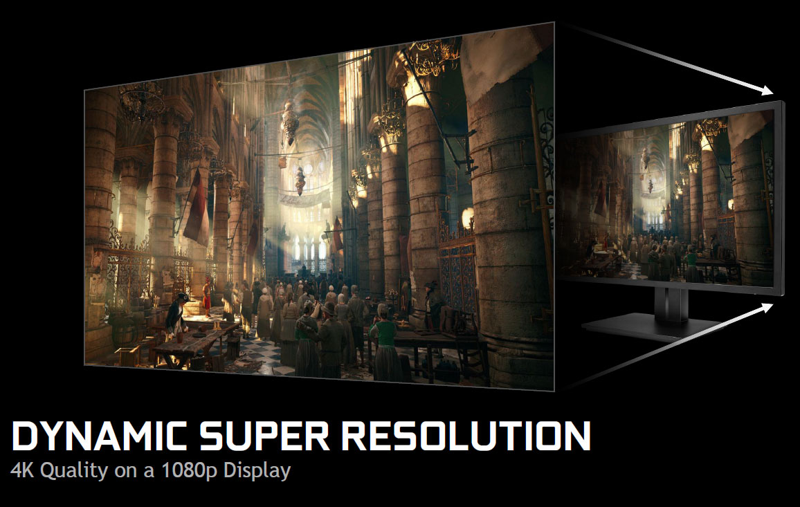

No new NVIDIA GPU architecture launch is complete without advancements in post-processing, particularly anti-aliasing. NVIDIA introduced an interesting feature called Dynamic Super Resolution (DSR), which it claims offers "4K-like clarity on a 1080p display". To us, it comes across as a really nice super-sampling AA algorithm with a filter.


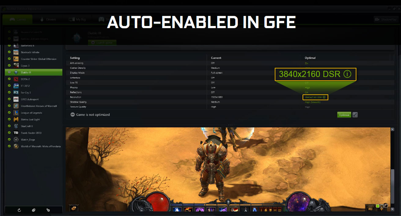
Using GeForce Experience, you can enable DSR arbitrarily for 3D apps. The other new algorithm is MFAA (multi-frame sampled AA), which offers MSAA-like image quality at a deficit of 30 percent in performance. Using GeForce Experience, MFAA can hence be substituted for MSAA, perhaps even arbitrarily.


Moving on, NVIDIA introduced VR Direct, a technology designed for the re-emerging VR headset market, due to the growing interest in Facebook's Occulus Rift VR headset. VR Direct is an API designed to reduce latency between the headset's input and the change on the display, governed by the principle that head movements are more rapid and unpredictable than pointing and clicking with a mouse.
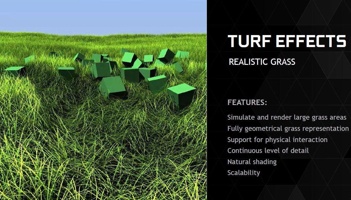

To meet the need of a low-cost (performance cost), realistic hair- or grass-rendering technology, NVIDIA came up with Turf Effects. NVIDIA PhysX also got a much needed feature-set update that introduces new gas dynamics and fluid adhesion effects. Epic's Unreal Engine 4 will implement the technology.
GeForce Experience
With its GeForce 320.18 WHQL drivers, NVIDIA released the first stable version of GeForce Experience. The application simplifies the process of configuring a game and is meant for PC gamers who aren't well-versed in all the necessary technobabble required to get a game to run at the best-possible settings with the hardware available to them. GeForce Experience is aptly named as it completes the experience of owning a GeForce graphics card; PCs, being the best-possible way to play video games, should not be any harder to use than gaming consoles.
NVIDIA Shadow Play
GeForce Experience Shadow Play is another feature NVIDIA recently debuted. Shadow Play lets you record gaming footage or stream content in real time, with a minimal performance drop to the game you're playing. The feature is handled by GeForce Experience, which lets you set hot-keys to toggle recording on the fly; or set output, format, quality, etc.
Unlike other apps, which record videos in loss-less AVI formats by tapping into the DirectX pipeline and clogging the system bus, disk, and memory with high bit-rate video streams, Shadow Play taps into a proprietary path that lets it copy the display output to the GPU's hardware H.264 encoder. This encoder neither strains the CPU nor the GPU's own unified shaders. Since the video stream being saved to a file comes out encoded, its bit-rate is infinitesimally lower than uncompressed AVI.
Our Patreon Silver Supporters can read articles in single-page format.
May 3rd, 2024 14:44 EDT
change timezone
Latest GPU Drivers
New Forum Posts
- 7800x3d $216 in bundle at Microcenter (37)
- Ryzen 7800x3d $196 with bundle at Microcenter (0)
- Announcement: VPN's no longer work right in Windows 10 or 11 or Servers (19)
- Old high quality PSU, or semi-old mid-quality PSU? (56)
- Is this Sapphire PULSE RX 5600 XT legit or fake? (37)
- fastest usb cable /transfer (15)
- Alphacool CORE 1 CPU block - bulging with danger of splitting? (72)
- 7900 XTX Seriously lacking (112)
- My Laptop is having issues with PL2 and EDP OTHER (5)
- TPU's Rosetta Milestones and Daily Pie Thread (1869)
Popular Reviews
- HYTE THICC Q60 240 mm AIO Review
- ASRock NUC BOX-155H (Intel Core Ultra 7 155H) Review
- Meze Audio LIRIC 2nd Generation Closed-Back Headphones Review
- Montech Sky Two GX Review
- Ugreen NASync DXP4800 Plus Review
- Upcoming Hardware Launches 2023 (Updated Feb 2024)
- Team Group T-Force Vulcan ECO DDR5-6000 32 GB CL38 Review
- MOONDROP x Crinacle DUSK In-Ear Monitors Review - The Last 5%
- AMD Ryzen 7 7800X3D Review - The Best Gaming CPU
- Logitech G Pro X Superlight 2 Review - Updated with 4000 Hz Tested
Controversial News Posts
- Intel Statement on Stability Issues: "Motherboard Makers to Blame" (234)
- Windows 11 Now Officially Adware as Microsoft Embeds Ads in the Start Menu (167)
- Sony PlayStation 5 Pro Specifications Confirmed, Console Arrives Before Holidays (117)
- AMD's RDNA 4 GPUs Could Stick with 18 Gbps GDDR6 Memory (114)
- AMD to Redesign Ray Tracing Hardware on RDNA 4 (111)
- NVIDIA Points Intel Raptor Lake CPU Users to Get Help from Intel Amid System Instability Issues (106)
- AMD "Strix Halo" Zen 5 Mobile Processor Pictured: Chiplet-based, Uses 256-bit LPDDR5X (103)
- AMD Ryzen 9 7900X3D Now at a Mouth-watering $329 (103)