Friday, March 16th 2012

GK104 Block Diagram Explained

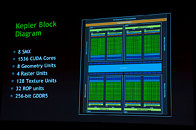
Specifications sheets of NVIDIA's GK104 GPU left people dumbfounded at the CUDA core count, where it read 1536, a 3-fold increase over that of the GeForce GTX 580 (3x 512). The block-diagram of the GK104, photographed at the NVIDIA press-meet by an HKEPC photographer, reveals how it all adds up. The GK104 is built on 28 nm fab process, with a die area of around 295 mm², according to older reports. Its component hierarchy essentially an evolution of that of the Fermi architecture.

The hierarchy starts with the GigaThread Engine, which marshals all the unprocessed and processed information between the rest of the GPU and the PCI-Express 3.0 system interface, below this, are four graphics processing clusters (GPCs), which holds one common resource, the raster engine, and two streaming multiprocessors (SMs), only this time, innovation has gone into redesigning the SM, it is called SMX. Each SMX has one next-generation PolyMorph 2.0 engine, instruction cache, 192 CUDA cores, and other first-level caches. So four GPCs of two SMXs each, and 16 SMXs of 192 CUDA cores each, amount to the 1536 CUDA core count. There are four raster units (amounting to 32 ROPs), 8 geometry units (each with a tessellation unit), and some third-level cache. There's a 256-bit wide GDDR5 memory interface.
Source: HKEPC
Add your own comment

23 Comments on GK104 Block Diagram Explained

#1
the54thvoid
Intoxicated Moderator
Wish I knew what that all actually meant...:wtf:
Posted on Reply
#2
KainXS
I think they made a good decision to cut individual core performance to fit more SP's in each SM, they did the same thing when they moved from the GT2XX series to the GT4XX series and it was worth it, and 1000Mhz stock is really suprising, I wonder what problems they ran into with the GK100 to prevent a release(Knowing Nvidia there just milking the market cause they know they have the faster cards maybe but oh well)
Posted on Reply
#3
Casecutter
btarunrGK104 GPU left people dumbfounded... essentially an evolution of that of the Fermi architecture. There's a 256-bit wide GDDR5 memory interface.
That's what I got from it! :eek:
Posted on Reply
#5
Shihab
the54thvoidWish I knew what that all actually meant...:wtf:
Fermi is a V4 engine with 4 huge cylinders.
Kepler is a V8 with smaller ones..

I think....
Posted on Reply
#6
Benetanegia
Hmm so it's 192 SPs per SM(X), that's how they got to bundle so many of them. Plenty of warp schedulers and dispatchers to feed them too. I think it's a very sleek design, we'll have to wait and see what the efficiency is though and one downside is a relatively very small L1 cache.
Posted on Reply
#7
Casecutter
MySchizoBuddyit means it is slightly better than 7970
But you need to include those new "star" (that btarunr's word for it, not mine) technologies TXAA, Adaptive V-Sync which gives that "organic" framerate feel! What kinds of fertilizers are used for organic farming?
What was the Cheech and Chong routine about "feel"… feels like…
Posted on Reply
#8
btarunr
Editor & Senior Moderator
It's a kickass GPU.

I hope I put it simple enough.
BenetanegiaHmm so it's 192 SPs per SM(X), that's how they got to bundle so many of them. Plenty of warp schedulers and dispatchers to feed them too. I think it's a very sleek design, we'll have to wait and see what the efficiency is though and one downside is a relatively very small L1 cache.
I'm hearing apart from high parallelization at the scheduler level, each small set of cores (lower level set than SMX) has a performance clock/voltage domain of its own. So not all 1536 CUDA cores will be running at the same clock speed (unless there's maximum or bare-minimum load). There will be hundreds of them running at countless combinations of clocks and voltages. It's as if the GPU knows exactly how much energy each single hardware resource needs at a given load.
Posted on Reply
#9
TheoneandonlyMrK
looks to be better then i expected, 4x setup and geometry engines and 8x total polymorph sounds like they may indeed pip the AMD crew this round , very modular too which should allow them(through binning) to have a reasonable range out quite quickly ,no mention of tesselation engines(fermi had 16 i think) ,have they incorporated that into their polymorph v2 or something
Posted on Reply
#10
Benetanegia
btarunrI'm hearing apart from high parallelization at the scheduler level, each small set of cores (lower level set than SMX) has a performance clock/voltage domain of its own. So not all 1536 CUDA cores will be running at the same clock speed (unless there's maximum or bare-minimum load). There will be hundreds of them running at countless combinations of clocks and voltages. It's as if the GPU knows exactly how much energy each single hardware resource needs at a given load.
That's amazing. Any word on what's the minimum set that can be disabled? I thought that an entire SMX? But with such control over clocks and voltage it could be a lower level I guess.

BTW that opens up an amazing oportunity for harvesting parts for the second SKU, though I'm not sure they'd do it or if it is desirable for us. Instead of requiring to clock (and voltage) the entire chip to the lower common denominator, it may be posible for them to clock only the parts that do not meet requirements lower, while the ones that can clock "normally" (high) could remain at the highest clock. It could be hard to implement and maybe even harder to make a SKU out of it, but on the tech level it would be amazing.
Posted on Reply
#11
Casecutter
btarunrhas a performance clock/voltage domain of its own. So not all 1536 CUDA cores will be running at the same clock speed (unless there's maximum or bare-minimum load)
Ok that's something... if they built into the chip level the idea of using Dynamic profiles or Adaptive V-Sync to shut down sections of cuda cores and are less dependent on just changing to core clock dramatically... this may as said be a "game changer" if Nvidia really implemented and made it integral at the chip level... they may have had this from the start, and not just some hocus pocus afterthought!
Posted on Reply
#12
deleted
BenetanegiaThat's amazing. Any word on what's the minimum set that can be disabled? I thought that an entire SMX? But with such control over clocks and voltage it could be a lower level I guess.

BTW that opens up an amazing oportunity for harvesting parts for the second SKU, though I'm not sure they'd do it or if it is desirable for us. Instead of requiring to clock (and voltage) the entire chip to the lower common denominator, it may be posible for them to clock only the parts that do not meet requirements lower, while the ones that can clock "normally" (high) could remain at the highest clock. It could be hard to implement and maybe even harder to make a SKU out of it, but on the tech level it would be amazing.
i doubt they will disable less than an sm at a time. if the difference in hardware between two skus is less than 10 percent, then the difference in performance is almost guaranteed to be even less than that. no one is going to spend another 50 bucks to get 3 or 4 more fps.

also, the chance of independently setting the max clock rate for each sm is exactly nil. it might make for marginally higher yields, but it would be a net loss in productivity because of all of the testing that would have to occur. it would also pretty much kill overclocking. imagine trying to oc a card with 20 different clock speed sliders 20 separate voltage tables.
Posted on Reply
#13
Benetanegia
deletedi doubt they will disable less than an sm at a time. if the difference in hardware between two skus is less than 10 percent, then the difference in performance is almost guaranteed to be even less than that. no one is going to spend another 50 bucks to get 3 or 4 more fps.
2 words: Lower clocks.
also, the chance of independently setting the max clock rate for each sm is exactly nil. it might make for marginally higher yields, but it would be a net loss in productivity because of all of the testing that would have to occur.
That is a valid point, requiring to have some kind of "profile" or qualification for each SM could be hard, which is why I did say it could be hard, but considering the huge amount of control that they already put there, I don't think it would be tremendously far-fetched to think about some kind of hardware automation for the next iteration, so that each SM can find (and report) its best clock and use the best voltage accordingly (if it does not do that already).

Anyway, I already questioned the feasibility of my comment regarding the posible SKUs. But tbh they could still make SKU based on "average" clock or average performance or something like that.

An example: imagine that the chip only had 2 SMs: 1 SM capable of 900 Mhz, 1 SM 1000 Mhz

1) Under normal conditions it would be a 900 Mhz SKU, because you have to limit the card to the lowest common denominator.
2) With dynamic clocking maybe it could be a 950 Mhz SKU, because that's the average clock both SMs would be running. Each chip would be different, but of course stock performance would be limited to a certain level, and that already occurs on current cards anyway.
it would also pretty much kill overclocking. imagine trying to oc a card with 20 different clock speed sliders 20 separate voltage tables.
Eehh... you didn't read what Btarunr said, right? You don't have to do anything, the chip does it by itself. You don't have to do 20 different sliders. There's just a main one like always and the chip finds which is best for each SM at any given time.
Posted on Reply
#14
ensabrenoir
Sound simply amazing......:eek:...fingers crossed that they actually deliver and its not all theory.... Future looking much greener. So gonna build something needlessly and senselessly over powered because... THE TECH IS THERE
Posted on Reply
#15
TheoneandonlyMrK
BenetanegiaBTW that opens up an amazing oportunity for harvesting parts for the second SKU, though I'm not sure they'd do it or if it is desirable for us. Instead of requiring to clock (and voltage) the entire chip to the lower common denominator, it may be posible for them to clock only the parts that do not meet requirements lower, while the ones that can clock "normally" (high) could remain at the highest clock. It could be hard to implement and maybe even harder to make a SKU out of it, but on the tech level it would be amazing.
thats what i had just said:rolleyes:

:wtf:So let me get this right by all indications you can oc the gpu core parts (thatll just be the 4x setup and polymorphx8?) ,if there is any more oc headroom but in all likely hood wont be able to adjust shader speed:wtf: or its likely to be ineffective in that they may downclock anyway, me personally im not so keen on redundancy, max all the way every day :)

jebus wizz ,throw us a bone gdam it ,thumbs up to that cookie or not;)
Posted on Reply
#16
Crap Daddy
theoneandonlymrkthats what i had just said:rolleyes:

:wtf:So let me get this right by all indications you can oc the gpu core parts (thatll just be the 4x setup and polymorphx8?) ,if there is any more oc headroom but in all likely hood wont be able to adjust shader speed:wtf: or its likely to be ineffective in that they may downclock anyway, me personally im not so keen on redundancy, max all the way every day :)

jebus wizz ,throw us a bone gdam it ,thumbs up to that cookie or not;)
Have a look at this link:

imgur.com/a/aQmuA#6n7nC

Here you'll find slides that I think were not posted here such as something about... overclocking!
Posted on Reply
#17
deleted
BenetanegiaEehh... you didn't read what Btarunr said, right? You don't have to do anything, the chip does it by itself. You don't have to do 20 different sliders. There's just a main one like always and the chip finds which is best for each SM at any given time.
I did read what he said. What I was referring to is what you were talking about here:
An example: imagine that the chip only had 2 SMs: 1 SM capable of 900 Mhz, 1 SM 1000 Mhz

1) Under normal conditions it would be a 900 Mhz SKU, because you have to limit the card to the lowest common denominator.
2) With dynamic clocking maybe it could be a 950 Mhz SKU, because that's the average clock both SMs would be running. Each chip would be different, but of course stock performance would be limited to a certain level, and that already occurs on current cards anyway.
There's no way for the GPU to know at what clocks and voltages its stable. You have to test it and figure it out and tell it. If you're trying to overclock a card with asymmetrical maximum clock speeds and voltages, you're going to have to figure out the best clock and voltage for each SM. That's simply unfeasible. The way it's going to work is that you will determine a single max clock speed and voltage for the card, and it will underclock itself when it determines that it doesn't need the additional processing power.
Posted on Reply
#18
Benetanegia
deletedThere's no way for the GPU to know at what clocks and voltages its stable. You have to test it and figure it out and tell it. If you're trying to overclock a card with asymmetrical maximum clock speeds and voltages, you're going to have to figure out the best clock and voltage for each SM. That's simply unfeasible.
I'm not talking about OC, as in users OCing the cards, I never did. I'm talking about factory profiles and yes they are feasible.
The way it's going to work is that you will determine a single max clock speed and voltage for the card, and it will underclock itself when it determines that it doesn't need the additional processing power.
Kepler cards already do much more than that according to the info revealed, which once again makes me think that you have not read about it. When the card detects that power consumption is lower than a previously set value, it overclocks/ovevlots itself until the limit is reached.

The user, yes, only sets a base clock and voltage and the GPu sets a maximum boost clock based on that, then it goes up or down as required by GPU load and power consumption.
Posted on Reply
#19
NHKS
If u want to see some slides i found for nV's GPU boost follow this link to post

& a rough comparison of power consumption bet. 7970 & 680, follow this link
Posted on Reply
#20
sergionography
thats very interesting, tho it seems on par with 7970 without this fancy dynamic clock thing
7970 has a good 30% overclock headroom but you have to do it manually , nvidia will do so when needed
im assuming you will be able to set maximum clock rate on the kepler and it will max out when needed
kinda similar to turbo mode in cpus
tho setting a certain clock at all times might change everything
that being said im sure its gonna be tricky to review this thing! but cant wait to see the real benchmarks and how the kepler cores perform without that dynamic clock trick
Posted on Reply
#21
sic_doni
:confused:
the54thvoidWish I knew what that all actually meant...:wtf:
so am I..hope I can read what all that means...:cry:
Posted on Reply
#22
Depth
btarunrThe hierarchy starts with the GigaThread Engine, which marshals all the unprocessed and processed information between the rest of the GPU and the PCI-Express 3.0 system interface, below this, are four graphics processing clusters (GPCs), which holds one common resource, the raster engine, and two streaming multiprocessors (SMs), only this time, innovation has gone into redesigning the SM, it is called SMX. Each SMX has one next-generation PolyMorph 2.0 engine, instruction cache, 192 CUDA cores, and other first-level caches. So four GPCs of two SMXs each, and 16 SMXs of 192 CUDA cores each, amount to the 1536 CUDA core count. There are four raster units (amounting to 32 ROPs), 8 geometry units (each with a tessellation unit), and some third-level cache.
Oh, right.
Posted on Reply
Add your own comment
Apr 26th, 2024 23:48 EDT change timezone

New Forum Posts

Popular Reviews

Controversial News Posts