Tuesday, September 12th 2006
SAMSUNG Announces First 40-nanometer 32 Gb NAND Flash Device
The new CTF-based NAND flash memory increases the reliability of the memory by sharply reducing inter-cell noise levels. Its surprisingly simple structure also enables higher scalability which will eventually improve manufacturing process technology from 40 nm to 30 and even 20nm.
In each 32Gb device, the control gate in the CTF is only 20 percent as large as a conventional control gate in a typical floating gate structure. With CTF, there is no floating gate. Instead, the data is temporarily placed in a "holding chamber" of the non-conductive layer of the flash memory composed of silicon nitride (SiN). This results in a higher level of reliability and better control of the storage current.
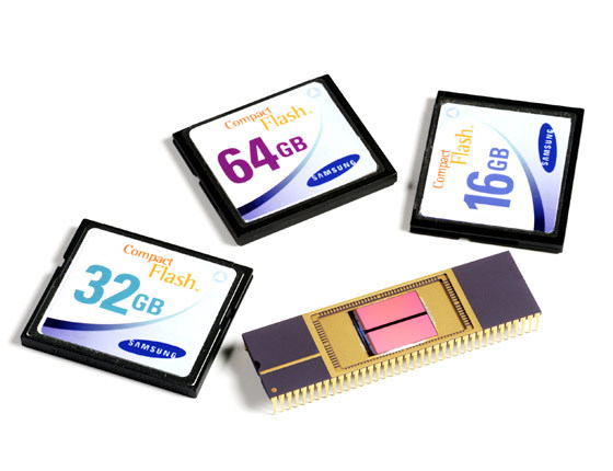
The 32Gb NAND flash memory can be used in memory cards with densities of up to 64-Gigabytes (GBs). One 64GB card can store over 64 hours of DVD resolution movies (40 movies) or 16,000 MP3 music files (1,340 hours).
The CTF design is enabled through the use of a TANOS structure comprised of tantalum (metal), aluminum oxide (high k material), nitride, oxide and silicon. The use of a TANOS structure marks the first application of a metal layer coupled with a high k material to the NAND device.
The TANOS CTF architecture, which serves as the foundation of the 40nm 32Gb CTF NAND flash announced today, was developed after extensive research of the Samsung Semiconductor R&D department. Samsung first revealed the TANOS structure through a paper at the 2003 International Electron Devices Meeting (IEDM).
The new 32Gb CTF memory was announced at the sixth annual Samsung press conference in Seoul.
Introduction of a 40nm manufacturing process for 32Gb NAND flash marks the seventh generation of NAND flash that follows the New Memory Growth Theory of double-density growth every 12 months, which was first presented by Dr. Chang Gyu Hwang, president and CEO of Samsung Electronics' Semiconductor Business in a keynote address at ISSCC 2002.
2 Comments on SAMSUNG Announces First 40-nanometer 32 Gb NAND Flash Device
Someday... I will carry the entire contents of my computer in my pocket.