Friday, May 27th 2016

NVIDIA GeForce GTX 1070 Reference PCB Pictured

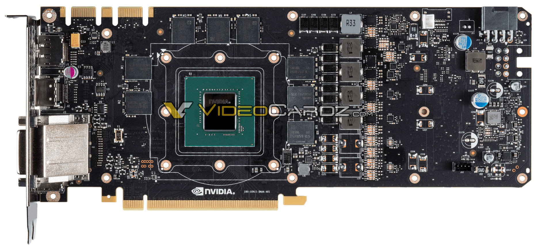
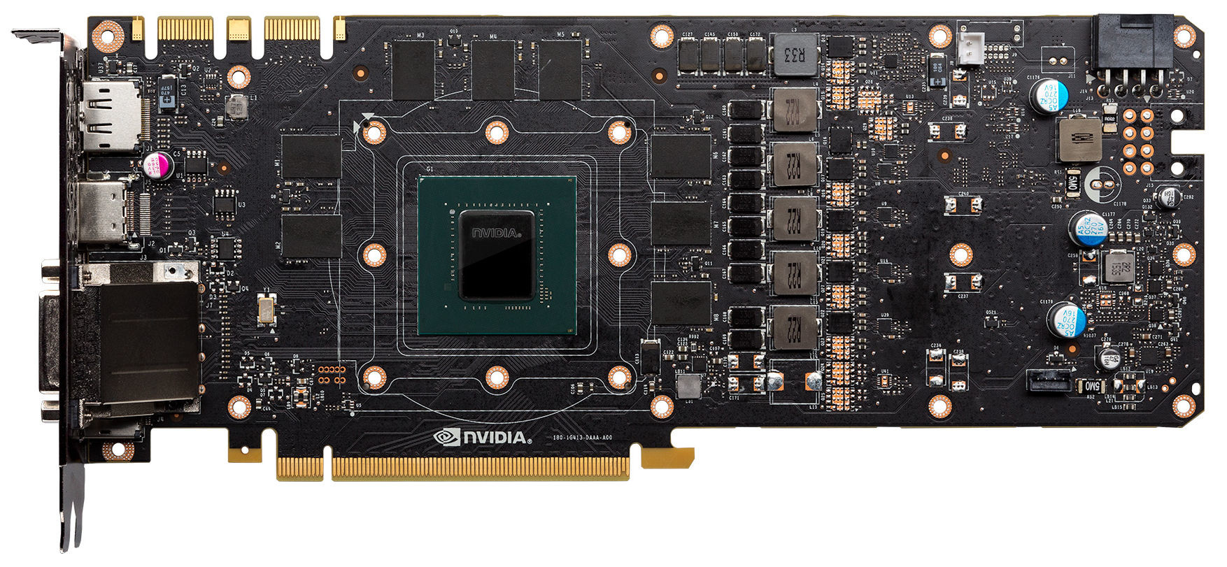
Here's the first picture of an NVIDIA reference-design PCB for the GeForce GTX 1070. The PCB (PG411) is similar to that of the GTX 1080 (PG413), except for two major differences, VRM and memory. The two PCBs are pictured below in that order. The GTX 1070 PCB features one lesser VRM phase compared to the GTX 1080. The other major difference is that it features larger GDDR5 memory chips, compared to the smaller GDDR5X memory chips found on the GTX 1080. These are 8 Gbps chips, and according to an older article, its clock speed is maxed out to specifications, at which the memory bandwidth works out to be 256 GB/s. The GeForce GTX 1070 will be available by 10th June.
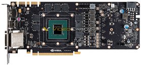
Source: VideoCardz
Add your own comment

37 Comments on NVIDIA GeForce GTX 1070 Reference PCB Pictured

#26
vega22
i wonder if nv are limiting how much they make custom cards ocable again?
Posted on Reply
#27
sweet
newtekie1I kind of figured it would be basically the same as the GTX1080 PCB, but with a few(VRM) components removed. Going from 5 Phase to 4 Phase.


The thing is that the amount of memory bandwidth per CUDA core is actually higher on the GTX1070 than the GTX1080.

GTX1080 = 320Gbps / 2560 = 128Mbps per CUDA Core
GTX1070 = 256Gbps / 1920 = 136.5Mbps per CUDA Core

Just food for thought.

Simply throwing more memory bandwidth at a GPU is not always going to yield better performance. AMD has been trying that strategy for generations, and it obviously isn't working. If the GPU itself can't process any faster, then the extra memory bandwidth goes wasted. So the GTX1080, with its roughly 25% faster GPU, can probably benefit from the higher memory bandwidth. While the slower GTX1070 probably wouldn't benefit that much from the higher memory bandwidth.
The cut out GPUs such as 1070 or 390 don't work like that. The scheduler still reserves space for the disabled SMs, coz they were cut off non-uniformly. Therefore the bandwidth per core isn't linear like in your math.
Posted on Reply
#28
newtekie1
Semi-Retired Folder
sweetThe cut out GPUs such as 1070 or 390 don't work like that. The scheduler still reserves space for the disabled SMs, coz they were cut off non-uniformly. Therefore the bandwidth per core isn't linear like in your math.
If you think that is true, you must think nVidia has some of the worst engineers in the world building their chips...

Just for knowledge, the Schedulers have moved to the SMs, I believe this started in Fermi. So each SM is responsible for issuing its own math instructions as well as its own memory load/store requests. When an SM is disabled, so it the schedulers in it. There is no reserving of memory bandwidth for SMs that aren't active, because the schedulers that would be trying to use that bandwidth are disabled as well.

Furthermore, how you explained it is not how a scheduler works even if they aren't included in the SMs. The scheduler receives memory load/store requests, and then it executes them in the order it feels best. It doesn't make request just sit there and wait because it hasn't heard from SM3 in a while and thinks it should reserve some time so SM3 can access the memory bus. If there are requests in the queue, it processes them as fast as it can.
Posted on Reply
#29
Jism
vega22i wonder if nv are limiting how much they make custom cards ocable again?
Yes that's called the OVP. It's on nvidia cards for a long time. It's called "over current protection" and it means that a chip is not able to exceed a certain amount of watts.

It has a few reasons, not to blow the interconnects of the PCB with a too high current going through, and making sure it does'nt get a shitload of dead cards in return because people OC'ed them extremely high.

AMD has them as well, inside their GPU's & CPU's. The CPU's have a bios setting that disabled the Overcurrent protection allowing you to make the CPU even consume more for higher clocks, but going past the OVP means that you can fry your CPU because of a too high current.

Oc'ers just solder their own VRM onto their GPU:


I wonder if that VRM on that card can be 're-enabled' by just solder the missing components on top of it.
Posted on Reply
#30
newtekie1
Semi-Retired Folder
JismYes that's called the OVP. It's on nvidia cards for a long time. It's called "over current protection" and it means that a chip is not able to exceed a certain amount of watts.

It has a few reasons, not to blow the interconnects of the PCB with a too high current going through, and making sure it does'nt get a shitload of dead cards in return because people OC'ed them extremely high.
Yeah, I think they started doing that when people started killing Fermi cards by cranking up the voltage, then complaining when things went bang...
Posted on Reply
#31
the54thvoid
Intoxicated Moderator
newtekie1Yeah, I think they started doing that when people started killing Fermi cards by cranking up the voltage, then complaining when things went bang...
A few cards offer the hardware option to disable the 'OVP'. The kingpin has solder points and I think the KFA2 HOF uber card had a switch which did the same. Needless to say, utilising either route invalidated warranties but it was an option for hardcore over clockers.
Posted on Reply
#32
moproblems99
ensabrenoir....once again everything nvidia(or intel) makes is over priced. Because as a company, they understand that their profit margin have to include r&d, future growth and development so they can continue producing performance leading tech? Its mind boggling to me..... given a Halo product will be overpriced because its a halo but do you want nvidia to just give stuff away? Struggle to survive...repackage old tech as new... we already know how this story ends.....
I would agree with you if we were talking about the X80Ti and whatever the new Titan will be but the X80 and X70 are now no longer halo products. Nvidia can price them whatever they want but it is concerning that a low-high range card is now $699. What is the Ti and Titan going to be? I can't believe they will lower the prices on these cards and release the Ti and Titan at $699 and $999.
Posted on Reply
#33
Fluffmeister
moproblems99I would agree with you if we were talking about the X80Ti and whatever the new Titan will be but the X80 and X70 are now no longer halo products. Nvidia can price them whatever they want but it is concerning that a low-high range card is now $699. What is the Ti and Titan going to be? I can't believe they will lower the prices on these cards and release the Ti and Titan at $699 and $999.
I would agree with you too, but the problem is the GP104 based GTX 1080 is the fastest thing available right now, and people appear to be lapping it up regardless of it's apparent expensiveness.... which frankly is just $50 more than the 980 Ti and Fury X launched at.

I'm not saying your observations are wrong, but it is just the reality of the current state of the market.

AMD are currently trying to flog a $1500 Radeon Pro Duo after all, Prosumer or not, the card makes zero sense right now.
Posted on Reply
#34
moproblems99
People can spend their money on crack and hookers for all I care, it's their prerogative. The 980 was also 10% to 20% faster than the 780Ti and it launched at $550USD. I could buy a 1080 if I want but frankly my 980 has been pissing me off since day one. Performance is great but I can't shake these damn TDRs and driver crashes. My CF 6850s were fine which drew more juice...whatever.

Anyway, I can't wait to revisit this conversationion when the 1180 Golden Founder's Edition is $799.
Posted on Reply
#35
erocker
*
Thread has been cleaned of off-topic posts. Please keep on topic and do so in a civil and amicable manner.

Thank you.
Posted on Reply
#36
[XC] Oj101
newtekie1I kind of figured it would be basically the same as the GTX1080 PCB, but with a few(VRM) components removed. Going from 5 Phase to 4 Phase.


The thing is that the amount of memory bandwidth per CUDA core is actually higher on the GTX1070 than the GTX1080.

GTX1080 = 320Gbps / 2560 = 128Mbps per CUDA Core
GTX1070 = 256Gbps / 1920 = 136.5Mbps per CUDA Core

Just food for thought.

Simply throwing more memory bandwidth at a GPU is not always going to yield better performance. AMD has been trying that strategy for generations, and it obviously isn't working. If the GPU itself can't process any faster, then the extra memory bandwidth goes wasted. So the GTX1080, with its roughly 25% faster GPU, can probably benefit from the higher memory bandwidth. While the slower GTX1070 probably wouldn't benefit that much from the higher memory bandwidth.
With the memory overclocked to 10 GHz it becomes an effective 170 MB/s per CUDA code, yet scaling isn't anywhere near what you'd expect. The GTX 1070 is not bandwidth starved, its bottleneck is GPU power.
Posted on Reply
#37
bug
ZoneDymoIf it does not make a difference, when why have it on the GTX1080? purely marketing?
GTX 1080 has more power. There's a chance the 1080 needs more than GDDR5 can deliver, while the 1070 does not. We don't know at this point, that's why I suggested we wait for reviews before burning Nvidia to the stake for using GDDR5 only.
Posted on Reply
Add your own comment
May 6th, 2024 02:21 EDT change timezone

New Forum Posts

Popular Reviews

Controversial News Posts