Wednesday, September 30th 2026
PCB Prototyping: From Design to PCBA with EasyEDA and JLCPCB
Learn how EasyEDA and JLCPCB connect PCB design, component sourcing, DFM, fabrication, and PCBA to simplify hardware prototyping. Modern electronic products increasingly demand smaller, denser, and more complex PCBs. High-speed interfaces, multilayer boards, HDI structures, rigid-flex designs, and fine-pitch components leave engineers with less room for manufacturing errors.
The challenge is not limited to PCB layout. Component availability, manufacturing constraints, fabrication requirements, and assembly specifications all have to stay aligned as the design evolves. A component may become unavailable after the layout is complete. A fabrication constraint may require a routing change. An assembly issue may only become apparent after manufacturing data has been prepared. Each additional handoff between design, sourcing, fabrication, and assembly creates another opportunity for data to become outdated. A more connected workflow can move these checks earlier in the development cycle. Design and Validate the PCB with EasyEDA
PCB design extends beyond layout. Engineers must account for component availability, design rules, manufacturability, and assembly needs while the design is still evolving. EasyEDA brings PCB design, component information, design verification, and collaboration into a browser-based environment.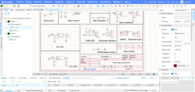 A Connected PCB Design Environment
EasyEDA provides browser-based schematic and PCB design, allowing engineers to create, review, and collaborate on projects without relying on a traditional desktop-only workflow.
Project sharing, version history, and access controls can help teams keep revisions organized. Supported Altium Designer and KiCad project and library formats can also be imported when engineers need to migrate existing designs.
EasyEDA Standard is suited to learning and less complex projects, while EasyEDA Pro provides additional capabilities for more advanced designs and team workflows.
Consider Component Availability During Design
Component selection can become a source of rework when availability is checked only after the PCB layout is finished. The JLCPCB component library is integrated into the design ecosystem, giving engineers access to component information while making design decisions. Checking availability earlier can reduce BOM, footprint, and routing changes later in the prototyping process.
Check Manufacturing Constraints Before Fabrication
DRC can identify common PCB layout issues before manufacturing, while JLCDFM reviews trace and spacing, solder-mask clearance, drilling, silkscreen, and assembly requirements.
Move from PCB Design to Manufacturing
Once the PCB layout has been reviewed, the design needs to be prepared for manufacturing.
A typical prototype requires a Gerber package, bill of materials (BOM), and component placement data (CPL). Engineers also need to verify the final manufacturing data, quantities, orientations, and specifications before placing an order.
These files can then move into the JLCPCB ordering workflow for PCB fabrication and assembly, reducing manual data transfer between separate platforms.
PCB Fabrication, Component Sourcing, and Assembly
Prototype manufacturing comes down to aligning PCB specs, components, assembly technology, inspection, and order quantity.
Multilayer PCB Fabrication
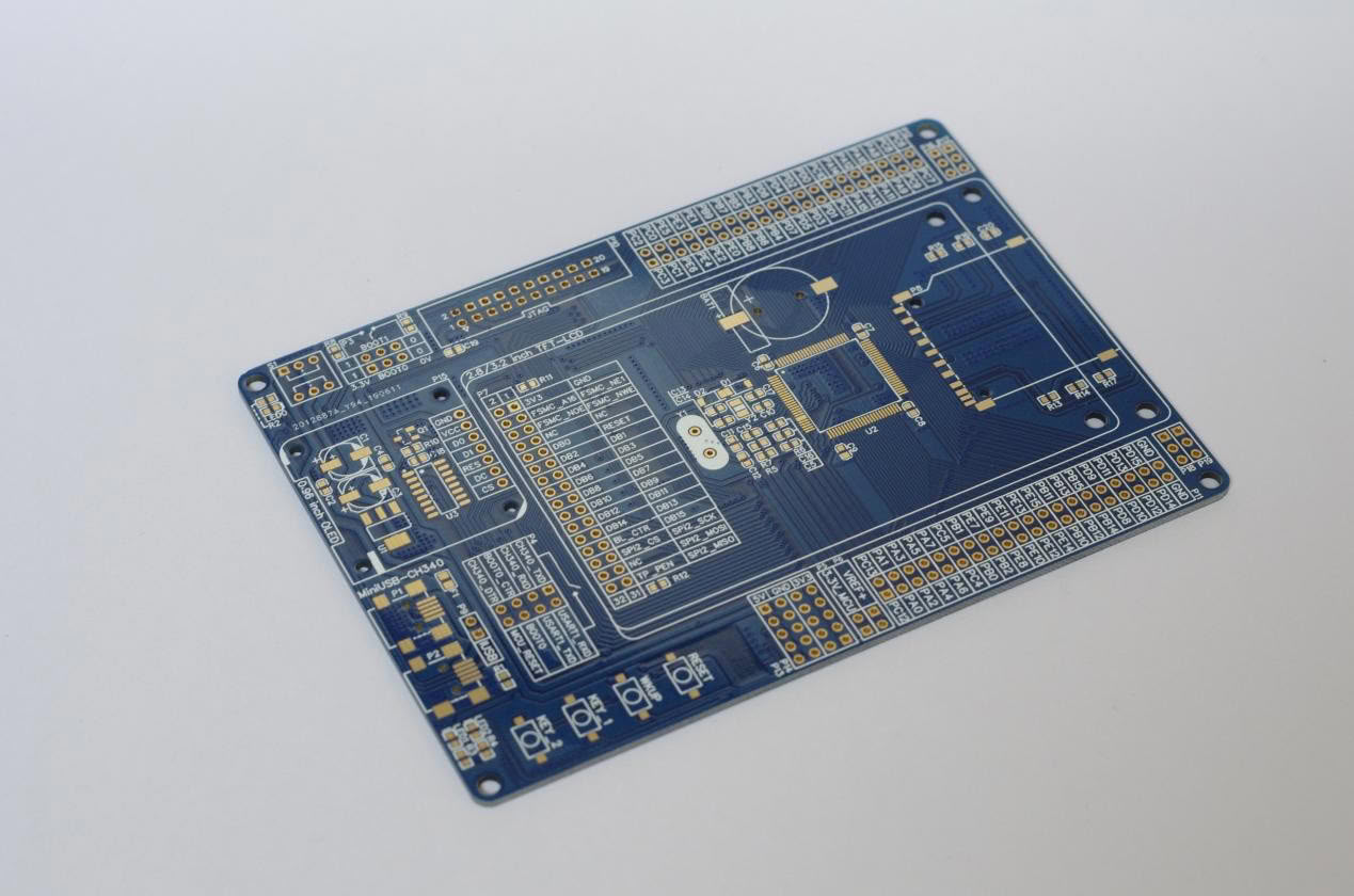
Multilayer PCB fabrication increases the number of variables that engineers need to consider, including layer count, stackup, feature dimensions, surface finish, and assembly requirements. JLCPCB supports PCB fabrication from 1 to 32 layers, with options including ENIG and other surface finishes for different application requirements.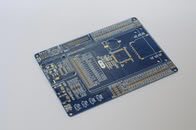 For designs using fine-pitch components, surface finish and pad geometry can directly affect assembly quality, so fabrication specifications should be considered together with the component and assembly requirements.
Component Sourcing for Prototype Builds
JLCPCB provides component sourcing options alongside PCB fabrication and assembly, allowing engineers to select available parts, source required components, or provide customer-supplied components for assembly.
For prototype builds, small quantities can support an iterative development process without requiring a large production run. Engineers can build an initial batch, test the hardware, and make revisions before moving to larger production quantities.
A shorter prototype turnaround can also help engineering teams move from design to physical testing sooner, accelerating validation and reducing delays between development iterations.
PCB Assembly for Fine-Pitch and Mixed-Technology Designs
PCB prototypes increasingly combine small SMD packages with connectors, through-hole components, and high-density devices.
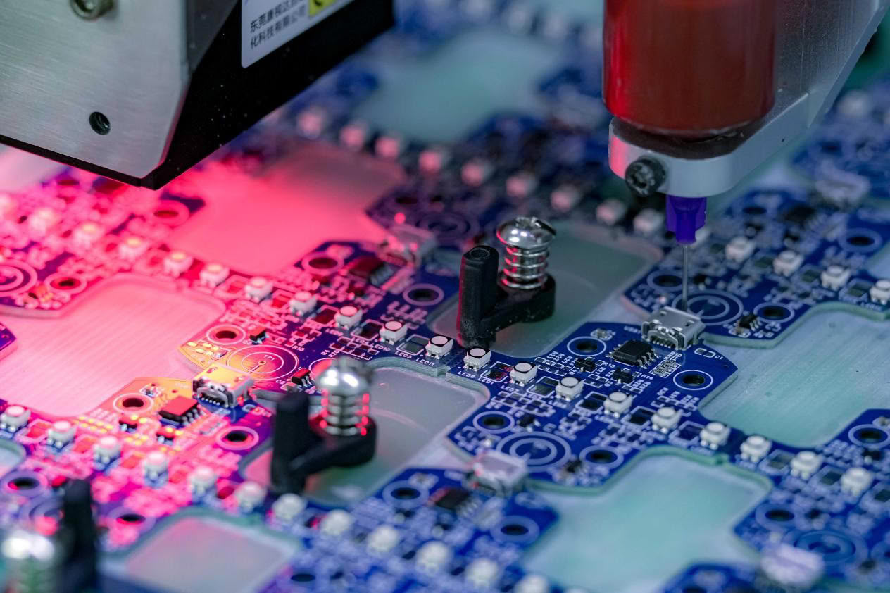
JLCPCB supports PCB Assembly across SMT, through-hole, and mixed-technology configurations, depending on the board and project requirements.
For more demanding assemblies, Standard PCBA supports packages including 0201 and 01005 components, BGA, and QFN, with published minimums of 0.35 mm IC pin spacing and 0.35 mm BGA pitch. Package selection still needs to account for routing, inspection, thermal requirements, and potential rework. A component that fits the electrical design may not necessarily be the easiest choice from a manufacturing perspective.
Inspection Before Hardware Bring-Up
Quality inspection is critical in prototype manufacturing. Depending on the service and package types, methods such as SPI, AOI, and X-ray inspection can help identify manufacturing defects before delivery. X-ray inspection can be used to check hidden solder joints, such as those found under BGA packages.
A More Connected PCB Prototyping Workflow
The value of a connected workflow is not simply having more tools. It is reducing unnecessary coordination between the stages that engineers already have to manage.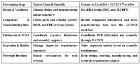 Reducing Friction Between Design and Manufacturing
 PCB prototyping involves more than fabricating a board. Component availability, manufacturing requirements, assembly, and inspection all need to stay aligned as a design moves toward physical validation.
EasyEDA, JLCDFM, and JLCPCB connect those stages: design validation, manufacturability checks, component sourcing, fabrication, assembly, and inspection run through one workflow instead of several. That cuts manual data transfers, reduces coordination overhead, and makes revisions easier to manage—with the short turnaround and low cost that keep an iterative cycle affordable.
The result is a shorter, more predictable path from PCB design to a tested, assembled prototype.
Request a PCB Quote to explore PCB fabrication and assembly options for your next prototype.
The challenge is not limited to PCB layout. Component availability, manufacturing constraints, fabrication requirements, and assembly specifications all have to stay aligned as the design evolves. A component may become unavailable after the layout is complete. A fabrication constraint may require a routing change. An assembly issue may only become apparent after manufacturing data has been prepared. Each additional handoff between design, sourcing, fabrication, and assembly creates another opportunity for data to become outdated. A more connected workflow can move these checks earlier in the development cycle.

PCB design extends beyond layout. Engineers must account for component availability, design rules, manufacturability, and assembly needs while the design is still evolving. EasyEDA brings PCB design, component information, design verification, and collaboration into a browser-based environment.
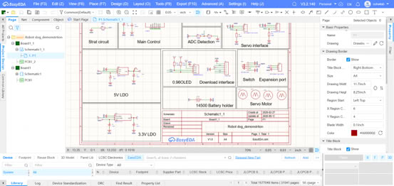
EasyEDA provides browser-based schematic and PCB design, allowing engineers to create, review, and collaborate on projects without relying on a traditional desktop-only workflow.
Project sharing, version history, and access controls can help teams keep revisions organized. Supported Altium Designer and KiCad project and library formats can also be imported when engineers need to migrate existing designs.
EasyEDA Standard is suited to learning and less complex projects, while EasyEDA Pro provides additional capabilities for more advanced designs and team workflows.
Consider Component Availability During Design
Component selection can become a source of rework when availability is checked only after the PCB layout is finished. The JLCPCB component library is integrated into the design ecosystem, giving engineers access to component information while making design decisions. Checking availability earlier can reduce BOM, footprint, and routing changes later in the prototyping process.
Check Manufacturing Constraints Before Fabrication
DRC can identify common PCB layout issues before manufacturing, while JLCDFM reviews trace and spacing, solder-mask clearance, drilling, silkscreen, and assembly requirements.
Move from PCB Design to Manufacturing
Once the PCB layout has been reviewed, the design needs to be prepared for manufacturing.
A typical prototype requires a Gerber package, bill of materials (BOM), and component placement data (CPL). Engineers also need to verify the final manufacturing data, quantities, orientations, and specifications before placing an order.
These files can then move into the JLCPCB ordering workflow for PCB fabrication and assembly, reducing manual data transfer between separate platforms.
PCB Fabrication, Component Sourcing, and Assembly
Prototype manufacturing comes down to aligning PCB specs, components, assembly technology, inspection, and order quantity.
Multilayer PCB Fabrication
Multilayer PCB fabrication increases the number of variables that engineers need to consider, including layer count, stackup, feature dimensions, surface finish, and assembly requirements. JLCPCB supports PCB fabrication from 1 to 32 layers, with options including ENIG and other surface finishes for different application requirements.
Component Sourcing for Prototype Builds
JLCPCB provides component sourcing options alongside PCB fabrication and assembly, allowing engineers to select available parts, source required components, or provide customer-supplied components for assembly.
For prototype builds, small quantities can support an iterative development process without requiring a large production run. Engineers can build an initial batch, test the hardware, and make revisions before moving to larger production quantities.
A shorter prototype turnaround can also help engineering teams move from design to physical testing sooner, accelerating validation and reducing delays between development iterations.
PCB Assembly for Fine-Pitch and Mixed-Technology Designs
PCB prototypes increasingly combine small SMD packages with connectors, through-hole components, and high-density devices.
JLCPCB supports PCB Assembly across SMT, through-hole, and mixed-technology configurations, depending on the board and project requirements.
For more demanding assemblies, Standard PCBA supports packages including 0201 and 01005 components, BGA, and QFN, with published minimums of 0.35 mm IC pin spacing and 0.35 mm BGA pitch.
Inspection Before Hardware Bring-Up
Quality inspection is critical in prototype manufacturing. Depending on the service and package types, methods such as SPI, AOI, and X-ray inspection can help identify manufacturing defects before delivery. X-ray inspection can be used to check hidden solder joints, such as those found under BGA packages.
A More Connected PCB Prototyping Workflow
The value of a connected workflow is not simply having more tools. It is reducing unnecessary coordination between the stages that engineers already have to manage.
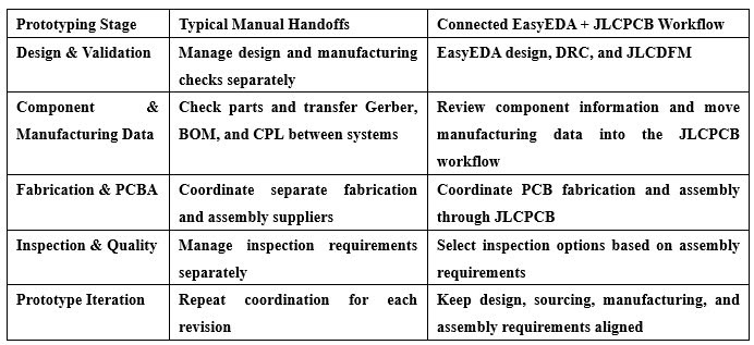
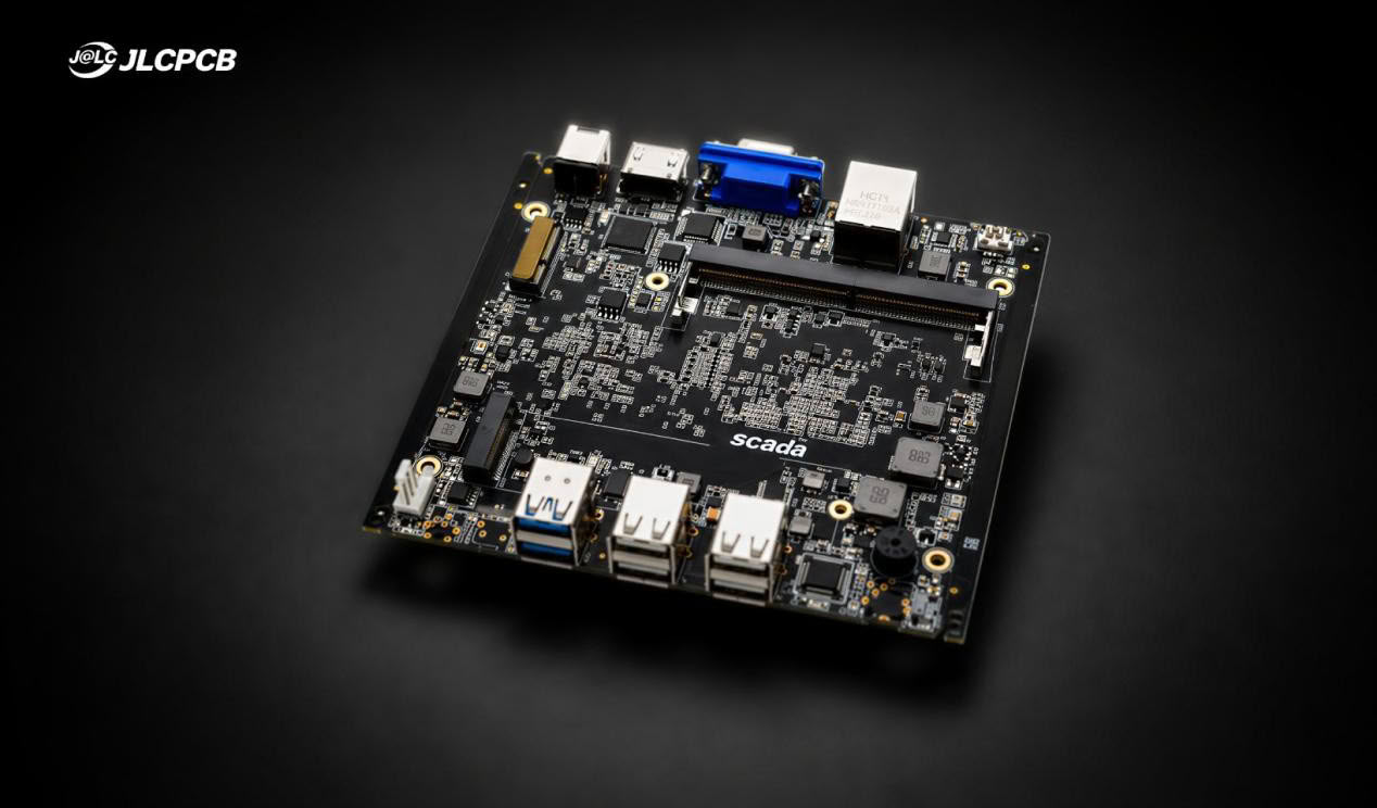
EasyEDA, JLCDFM, and JLCPCB connect those stages: design validation, manufacturability checks, component sourcing, fabrication, assembly, and inspection run through one workflow instead of several. That cuts manual data transfers, reduces coordination overhead, and makes revisions easier to manage—with the short turnaround and low cost that keep an iterative cycle affordable.
The result is a shorter, more predictable path from PCB design to a tested, assembled prototype.
Request a PCB Quote to explore PCB fabrication and assembly options for your next prototype.