Tuesday, March 24th 2009

RV790 Reaches 1.00 GHz, Indicates Overclocked SKUs in the Making
Following our report of ASUS preparing an overclocked Radeon HD 4890 accelerator with clock speeds well above 900 MHz (core) and 1000 MHz (memory), the possibility has come to surface that AMD has carved out a new range of Radeon HD 4890 accelerators from the unusually high overclocking headroom the RV790 GPU has. The credit also goes to the reference-design PCB, which is known to possess some of the highest quality digital PWM components to handle power, and 4 GT/s GDDR5 memory, which is now known to have a good overclocking headroom.
It has surfaced on the forums of Chinese tech community PCInLife, that the RV790 rather effortlessly reached the 1 GHz mark, the slider-limit of Catalyst Control Center, sparking off fresh rumors that AMD partners may be creating a fresh niche of highly-overclocked cards shortly after Radeon HD 4890 comes to be. The overclocker reached speeds of 1 GHz (core) and 1125 MHz (4.50 GHz effective, memory). At the said speeds, the card was put through 3DMark Vantage with its eXtreme settings. It churned-out a score of X5480, which puts its performance somewhere between those of the GeForce GTX 280 and GeForce GTX 285. It should also be taken into account that the drivers RV790 users the world over have been using, are preliminary beta drivers. AMD plans to release Catalyst 9.4 with the release of Radeon HD 4890, which just may impact positively on the performance of the product.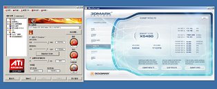 Factory-overclocked cards based on ATI Radeon have since now been a formality. Even cards with the iconic HIS IceQ TurboX branding, haven't been known to have high (~15~20%) increase in clock speeds. With this feat surfacing, it has been established that the RV790 holds the capability to reach some very high clock speeds. On course to the 1 GHz mark, the overclocker at PCInLife comfortably reached 925/1025 MHz (X5021) and 950/1075 MHz (X5202). It sounds plausible that these speeds could be the speeds factory-overclocked cards come at, with a branding system similar to what NVIDIA uses: a tier-1 (light overclock), tier-2 (moderate overclock), tier-3 (high overclock), and tier-4 (extreme overclock). At any rate, this is turning out to be an exciting fortnight for the high-end GPU industry.
Source:
PCInLife
It has surfaced on the forums of Chinese tech community PCInLife, that the RV790 rather effortlessly reached the 1 GHz mark, the slider-limit of Catalyst Control Center, sparking off fresh rumors that AMD partners may be creating a fresh niche of highly-overclocked cards shortly after Radeon HD 4890 comes to be. The overclocker reached speeds of 1 GHz (core) and 1125 MHz (4.50 GHz effective, memory). At the said speeds, the card was put through 3DMark Vantage with its eXtreme settings. It churned-out a score of X5480, which puts its performance somewhere between those of the GeForce GTX 280 and GeForce GTX 285. It should also be taken into account that the drivers RV790 users the world over have been using, are preliminary beta drivers. AMD plans to release Catalyst 9.4 with the release of Radeon HD 4890, which just may impact positively on the performance of the product.

103 Comments on RV790 Reaches 1.00 GHz, Indicates Overclocked SKUs in the Making
Originally Posted by iStink View Post
it takes AMD 1ghz to do what it takes nvidia 650mhz to do.
I understand there's differences in architecture, but doesn't a chip using a higher frequency need more voltage? And less voltage for more performance is where we want to go, not more voltage for equal amount of performance...
Still though, as always, amd will need to offer these cards at a killer price to compete with nvidia. Also, they aren't using havok in their drivers just yet. These preliminary tests show promise.
With ATi the core and shaders run at the same speed, with nVidia they don't. nVidia's shaders are way over 1GHz, and the shaders are the work horses.
your 100% right
It has been confirmed that the new chip has a larger die. That's probably to minimize inter-component leakages.
ATI fanbois running rampant like a all girl sleepover on redbull, and Nvidia fanbois proclaiming that the new chip is junk and will never be as precious as their rebadged hardware.
i kid of course ;)
Like btarunr mentioned, the rv790 will be bigger probably to minimize inter-component leakages and it will be built on a better 55mn process. The PCB will have better power circuitry too.
So even if the main voltage increases, that doesn't have to translate into a higher TDP or heat output at 850Mhz. That is, if they can drastically decrease leakage (which seems to be true).
bring on the GT212 dang it!
your saying its a different chip solely because the die size is different (all we know so far, AT A GLANCE)
what we actually know so far is it performs exactly as an equally clocked 4870 does, its a faster running RV770.
like i said, we "know" (from preliminaries) it performs the same as a 4870 at that speed, so really, what does it bring to the table except for higher speeds (which arent to be downplayed, everyone loves faster gear) whatever changes have been made on the CHIP serve to facilitate this speed, clock for clock we are seeing no benefits.
as you say its a different GPU carrying the same specs, so pretty much the same deal as GT200 to GT200b except in place of a shrink we have some minor tweaks.
I am a huge fan of the competition, and it would be nice to see this card force nvidias hand on pricing or a new card.
and @ Steevo, get used to it man, the better part of us are irrational when it comes to hardware. ATi lovers will always think their new unreleased GPU will tear nvidia limb from limb and it never really does, they compete well, as they should. just as nvidia fanboys think they can hold the crown forever, they cant, and it wouldn't be fun if they did.