
1
Cores
1
Threads
30 W
TDP
1200 MHz
Frequency
N/A
Boost
Tualatin
Codename
Socket 370
Socket

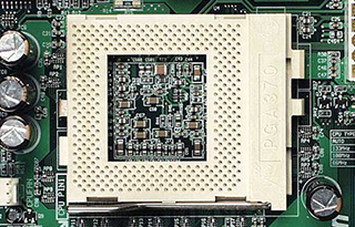
Intel Socket 370
The Intel Celeron 1200 was a desktop processor with 1 core, launched in October 2001, at an MSRP of $103. It is part of the Celeron lineup, using the Tualatin architecture with Socket 370. Celeron 1200 has 256 KB of L2 cache and operates at 1200 MHz. Intel is building the Celeron 1200 on a 130 nm production process using 44 million transistors. The multiplier is locked on Celeron 1200, which limits its overclocking capabilities.
With a TDP of 30 W, the Celeron 1200 consumes only little energy. The highest officially supported memory speed is 133 MT/s, but with overclocking (and the right memory modules) you can go even higher. Actual memory technology support depends on the chosen motherboard, because the memory controller is located on the motherboard (not in the processor). Although the processor doesn't come with integrated graphics, certain motherboards with compatible chipsets can provide this capability.
Many games will refuse to start on this processor due to the lack of the SSE2/SSE3/SSE4 instruction set.
Physical
| Socket: | Intel Socket 370 |
|---|---|
| Foundry: | Intel |
| Process Size: | 130 nm |
| Transistors: | 44 million |
| Die Size: | 80 mm² |
| Package: | µPGA |
| tCaseMax: | 70°C |
Processor
| Market: | Desktop |
|---|---|
| Production Status: | End-of-life |
| Release Date: | Oct 2001 |
| Launch Price: | $103 |
| Part#: | SL5XS SL5Y5 SL656 SL68P SL6C8 SL6JS SL6RP |
Performance
| Frequency: | 1200 MHz |
|---|---|
| Turbo Clock: | N/A |
| Base Clock: | 100 MHz |
| Multiplier: | 12.0x |
| Multiplier Unlocked: | No |
| Voltage: | 1.5 V |
| TDP: | 30 W |
Architecture
| Codename: | Tualatin |
|---|---|
| Generation: |
Celeron
(Tualatin) |
| Memory Support: |
unknown
Depends on motherboard |
| Rated Speed: | 133 MT/s |
| Memory Bus: | Single-channel |
| Northbridge Location: | Motherboard |
| ECC Memory: | No |
| Chipsets: | i815, i815e, VIA 694T, ALi M1651T, SiS 635T |
Core Config
| # of Cores: | 1 |
|---|---|
| # of Threads: | 1 |
| SMP # CPUs: | 1 |
| Integrated Graphics: | On certain motherboards (Chipset feature) |
Cache
| Cache L1: | 32 KB |
|---|---|
| Cache L2: | 256 KB |
Features
|
Notes
| Many S-Specs overlap in stepping code. Stepping table is as follows: Stepping A0 - SL5XS, SL5Y5, SL656, SL68P, SL6JS, Stepping B0 - SL6RP Stepping B1 - SL6JS, SL6C8 Stepping BA - SL6C8 |
Jun 15th, 2024 15:54 EDT
change timezone
Latest GPU Drivers
New Forum Posts
- A Final Fantasy IX Reminiscence - My love letter and homage to one of the best stories ever told (0)
- Intel Optane 1TB (1)
- System shutdown from short when connecting USB type C cable? (18)
- Alphacool - problem with radiators - bad fin soldering? (26)
- new tv/display what one? what to avoid? (19)
- Can you help me decide for which AM4 CPU to buy plz? (16)
- Your PC ATM (34632)
- Youtube benchmark,test of cpu,gpu using script (4)
- Ghetto Mods (4342)
- Black screen in SOME games 6800xt Sapphire Pulse (8)
Popular Reviews
- Aune AR5000 Headphones + S17 Pro Headphones Amplifier Review
- Pulsar Xlite V3 eS Review
- VAXEE Outset AX Wireless (4K) Review
- Upcoming Hardware Launches 2024 (Updated May 2024)
- Team Group T-Force G70 Pro 2 TB Review
- Intel Lunar Lake Technical Deep Dive - So many Revolutions in One Chip
- AMD Ryzen 7 7800X3D Review - The Best Gaming CPU
- NZXT H6 Flow RGB Review
- Quick Look: Final UX2000 Wireless Noise Canceling Headphones
- Thermal Grizzly KryoSheet Review - Tested on RX 7900 XTX with 475 W
Controversial News Posts
- Possible Specs of NVIDIA GeForce "Blackwell" GPU Lineup Leaked (132)
- NVIDIA RTX 5090 "Blackwell" Founders Edition to Implement the "RTX 4090 Ti" Cinderblock Design (118)
- AMD Outs Ryzen 5000XT Processors for Socket AM4, an 8-year Old Socket (105)
- Nightmare Fuel for Intel: Arm CEO Predicts Arm will Take Over 50% Windows PC Market-share by 2029 (105)
- AMD Ryzen 9000 Zen 5 Single Thread Performance at 5.80 GHz Found 19% Over Zen 4 (103)
- AMD Says Ryzen 9000 Series Won't Beat 7000X3D Series at Gaming (101)
- AMD Zen 5 Storms into Gaming Desktops with Ryzen 9000 "Granite Ridge" Processors (100)
- Biden Administration to Revive Trump-Era Tariffs on China-made GPUs and Motherboards (95)