 / Ryzen 5")
6
Cores
12
Threads
15 W
TDP
2.3 GHz
Frequency
4.3 GHz
Boost
Barcelo
Codename
Socket FP6
Socket

Front

Connectivity
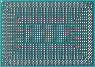
AMD Socket FP6
The AMD Ryzen 5 5625U is a mobile processor with 6 cores, launched in January 2022. It is part of the Ryzen 5 lineup, using the Zen 3 (Cezanne) architecture with Socket FP6. Thanks to AMD Simultaneous Multithreading (SMT) the core-count is effectively doubled, to 12 threads. Ryzen 5 5625U has 16 MB of L3 cache and operates at 2.3 GHz by default, but can boost up to 4.3 GHz, depending on the workload. AMD is making the Ryzen 5 5625U on a 7 nm production node using 10,700 million transistors. The silicon die of the chip is not fabricated at AMD, but at the foundry of TSMC. The multiplier is locked on Ryzen 5 5625U, which limits its overclocking potential.
With a TDP of 15 W, the Ryzen 5 5625U consumes very little energy. AMD's processor supports DDR4 memory with a dual-channel interface. The highest officially supported memory speed is 3200 MT/s, but with overclocking (and the right memory modules) you can go even higher. ECC memory is supported, too, which is an important capability for mission-critical systems, to avoid data corruption. For communication with other components in the computer, Ryzen 5 5625U uses a PCI-Express Gen 3 connection. This processor features the Radeon Vega 7 integrated graphics solution.
Hardware virtualization is available on the Ryzen 5 5625U, which greatly improves virtual machine performance. Programs using Advanced Vector Extensions (AVX) can run on this processor, boosting performance for calculation-heavy applications. Besides AVX, AMD is including the newer AVX2 standard, too, but not AVX-512.
Physical
| Socket: | AMD Socket FP6 |
|---|---|
| Foundry: | TSMC |
| Process Size: | 7 nm |
| Transistors: | 10,700 million |
| Die Size: | 180 mm² |
| Package: | FC-BGA1140 |
| tJMax: | 95°C |
Processor
| Market: | Mobile |
|---|---|
| Production Status: | Active |
| Release Date: | Jan 6th, 2022 |
| Part#: | 100-000000583 |
Performance
| Frequency: | 2.3 GHz |
|---|---|
| Turbo Clock: | up to 4.3 GHz |
| Base Clock: | 100 MHz |
| Multiplier: | 23.0x |
| Multiplier Unlocked: | No |
| TDP: | 15 W |
| Configurable TDP: | 25W |
Architecture
| Codename: | Barcelo |
|---|---|
| Generation: |
Ryzen 5
(Zen 3 (Cezanne)) |
| Memory Support: | DDR4 |
| LPDDR4x Speed: | 4267 MT/s |
| Rated Speed: | 3200 MT/s |
| Memory Bus: | Dual-channel |
| ECC Memory: | Yes |
| PCI-Express: |
Gen 3, 16 Lanes (CPU only) |
Core Config
| # of Cores: | 6 |
|---|---|
| # of Threads: | 12 |
| SMP # CPUs: | 1 |
| Integrated Graphics: | Radeon Vega 7 |
Cache
| Cache L1: | 64 KB (per core) |
|---|---|
| Cache L2: | 512 KB (per core) |
| Cache L3: | 16 MB (shared) |
Features
|
Notes
| Graphics engine boost clock: 1600MHz |
Apr 26th, 2024 17:40 EDT
change timezone
Latest GPU Drivers
New Forum Posts
- What's your latest tech purchase? (20354)
- 5800x (and other Zen 3 chips) PBO settings/Temperature fix (934)
- Only EDP Other in Core? (2)
- Alphacool CORE 1 CPU block - bulging with danger of splitting? (30)
- Dell Workstation Owners Club (3061)
- Xeon Owners Club (8700)
- Secure boot already open help (10)
- hacked (77)
- Best SSD for system drive (92)
- looking to build a new system and im considering asrock brand but i have some doubts/concerns. (4)
Popular Reviews
- HYTE THICC Q60 240 mm AIO Review
- MOONDROP x Crinacle DUSK In-Ear Monitors Review - The Last 5%
- Upcoming Hardware Launches 2023 (Updated Feb 2024)
- Alienware Pro Wireless Gaming Keyboard Review
- Thermalright Phantom Spirit 120 EVO Review
- FiiO K19 Desktop DAC/Headphone Amplifier Review
- ASUS Radeon RX 7900 GRE TUF OC Review
- Ugreen NASync DXP4800 Plus Review
- AMD Ryzen 7 7800X3D Review - The Best Gaming CPU
- Sapphire Radeon RX 7900 GRE Pulse Review
Controversial News Posts
- Windows 11 Now Officially Adware as Microsoft Embeds Ads in the Start Menu (135)
- Sony PlayStation 5 Pro Specifications Confirmed, Console Arrives Before Holidays (117)
- NVIDIA Points Intel Raptor Lake CPU Users to Get Help from Intel Amid System Instability Issues (106)
- AMD "Strix Halo" Zen 5 Mobile Processor Pictured: Chiplet-based, Uses 256-bit LPDDR5X (103)
- US Government Wants Nuclear Plants to Offload AI Data Center Expansion (98)
- AMD's RDNA 4 GPUs Could Stick with 18 Gbps GDDR6 Memory (95)
- Developers of Outpost Infinity Siege Recommend Underclocking i9-13900K and i9-14900K for Stability on Machines with RTX 4090 (85)
- Windows 10 Security Updates to Cost $61 After 2025, $427 by 2028 (84)