 / Ryzen 5")
6
Cores
12
Threads
28 W
TDP
3.5 GHz
Frequency
4.9 GHz
Boost
Hawk Point
Codename
Socket FP7
Socket

Front

Connectivity
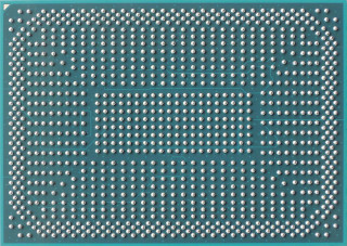
AMD Socket FP7
The AMD Ryzen 5 PRO 8640HS is a mobile processor with 6 cores, launched in April 2024. It is part of the Ryzen 5 lineup, using the Zen 4 (Hawk Point) architecture with Socket FP7. Thanks to AMD Simultaneous Multithreading (SMT) the core-count is effectively doubled, to 12 threads. Ryzen 5 PRO 8640HS has 16 MB of L3 cache and operates at 3.5 GHz by default, but can boost up to 4.9 GHz, depending on the workload. AMD is building the Ryzen 5 PRO 8640HS on a 4 nm production process using 25,000 million transistors. The silicon die of the chip is not fabricated at AMD, but at the foundry of TSMC. The multiplier is locked on Ryzen 5 PRO 8640HS, which limits its overclocking capabilities.
With a TDP of 28 W, the Ryzen 5 PRO 8640HS consumes only little energy. AMD's processor supports DDR5 memory with a dual-channel interface. The highest officially supported memory speed is 5600 MT/s, but with overclocking (and the right memory modules) you can go even higher. ECC memory is supported, too, which is an important capability for mission-critical systems, to avoid data corruption. For communication with other components in the machine, Ryzen 5 PRO 8640HS uses a PCI-Express Gen 4 connection. This processor features the Radeon 760M integrated graphics solution.
Hardware virtualization is available on the Ryzen 5 PRO 8640HS, which greatly improves virtual machine performance. Programs using Advanced Vector Extensions (AVX) will run on this processor, boosting performance for calculation-heavy applications. Besides AVX, AMD has added support for the newer AVX2 and AVX-512 instructions, too.
Physical
| Socket: | AMD Socket FP7 |
|---|---|
| Foundry: | TSMC |
| Process Size: | 4 nm |
| Transistors: | 25,000 million |
| Die Size: | 178 mm² |
| Package: | FP7, FP7r2 |
| tJMax: | 100°C |
Processor
| Market: | Mobile |
|---|---|
| Production Status: | Active |
| Release Date: | Apr 16th, 2024 |
| Part#: | 100-000001354 (FP7r2) , 100-000001382 (FP7) |
Performance
| Frequency: | 3.5 GHz |
|---|---|
| Turbo Clock: | up to 4.9 GHz |
| Base Clock: | 100 MHz |
| Multiplier: | 35.0x |
| Multiplier Unlocked: | No |
| XDNA NPU: | 16 TOPS |
| TDP: | 28 W |
| Configurable TDP: | 20-30 W |
Architecture
| Codename: | Hawk Point |
|---|---|
| Generation: |
Ryzen 5
(Zen 4 (Hawk Point)) |
| Memory Support: | DDR5 |
| LPDDR5x Speed: | 7500 MT/s |
| Rated Speed: | 5600 MT/s |
| Memory Bus: | Dual-channel |
| ECC Memory: | Yes |
| PCI-Express: |
Gen 4, 20 Lanes (CPU only) |
Core Config
| # of Cores: | 6 |
|---|---|
| # of Threads: | 12 |
| SMP # CPUs: | 1 |
| Integrated Graphics: | Radeon 760M |
Cache
| Cache L1: | 64 KB (per core) |
|---|---|
| Cache L2: | 1 MB (per core) |
| Cache L3: | 16 MB (shared) |
Features
|
Notes
| Graphics engine boost clock: 2600MHz |
Apr 29th, 2024 16:12 EDT
change timezone
Latest GPU Drivers
New Forum Posts
- What are you playing? (20557)
- Dialing in the overlock on my new 12600kf, matured silicon process showing great results... (33)
- 7900 XTX Seriously lacking (5)
- Is it better for zero RPM PSUs to place the fan on top? (27)
- Looking for recommendations to upgrade the GPU (31)
- Is this Sapphire PULSE RX 5600 XT legit or fake? (17)
- i7-1355U (6)
- Show us your collections thread!! (285)
- HTPC (0)
- Z790 ACE MAX? (6)
Popular Reviews
- Ugreen NASync DXP4800 Plus Review
- HYTE THICC Q60 240 mm AIO Review
- AMD Radeon RX 7800 XT Review
- Upcoming Hardware Launches 2023 (Updated Feb 2024)
- MOONDROP x Crinacle DUSK In-Ear Monitors Review - The Last 5%
- Thermalright Phantom Spirit 120 EVO Review
- AMD Ryzen 7 7800X3D Review - The Best Gaming CPU
- FiiO K19 Desktop DAC/Headphone Amplifier Review
- ASUS Radeon RX 7900 GRE TUF OC Review
- Logitech G Pro X Superlight 2 Review - Updated with 4000 Hz Tested
Controversial News Posts
- Windows 11 Now Officially Adware as Microsoft Embeds Ads in the Start Menu (150)
- Intel Statement on Stability Issues: "Motherboard Makers to Blame" (144)
- Sony PlayStation 5 Pro Specifications Confirmed, Console Arrives Before Holidays (117)
- NVIDIA Points Intel Raptor Lake CPU Users to Get Help from Intel Amid System Instability Issues (106)
- AMD's RDNA 4 GPUs Could Stick with 18 Gbps GDDR6 Memory (103)
- AMD "Strix Halo" Zen 5 Mobile Processor Pictured: Chiplet-based, Uses 256-bit LPDDR5X (103)
- US Government Wants Nuclear Plants to Offload AI Data Center Expansion (98)
- TechPowerUp Hiring: Reviewers Wanted for Motherboards, Laptops, Gaming Handhelds and Prebuilt Desktops (89)