GTX500 is a refresh of GTX400. Not much is changed at all. 10% higher clocks and GTX480 also had a shader cluster laser cut the same as GTX460 so they might have fixed that, though it doesn't seem likely otherwise it should be a helluva lot faster than testing is showing. In testing it is showing only a 4-10% improvement over GTX480 but if all the clocks are boosted 10%, that should account for the difference by itself. A 10% clock boost plus an additional shader cluster should be 20-25% faster, so something is still wrong with the Fermi picture. The extra shader cluster is either still locked or they found some way to unlock it but hobble them all so they aren't doing as much work as before. It's still mostly same GF100 core with a few efficiencies stolen from GF104 to reduce power and heat, that's all. Move along, nothing to see here.
Check your math and the reviews you read... :shadedshu
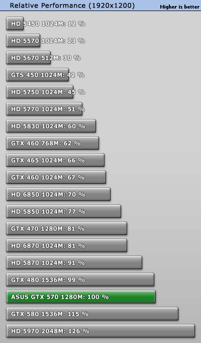
580 is 16% faster than 480 according to W1zzard's review, see:
Now, 512 SP is exactly 6.667% more shaders than 480 and GTX580 clocks are 10% faster than 480 (like you said):
10%+6%= 16% (16~17%).
That's perfect scaling and a far cry from the poor scaling that Cayman is showing: HD6970 should be 20% faster than HD 6950 (10% clock, ~10% shader count) and 30% faster than HD5870 to show the same scaling.
The truth is that none of them are using a new architecture for these "new" generation. GF110 is just a fixed GF100, it was never meant as a new chip (which was a huuuge dissapointment for me), but at least, GF100 was a completely new architecture with no resemblance to any previous GPU and, at least for now, it scales 100% as SP count or clocks are increased. If previous generations are something to go by, Fermi will easily scale to 1024 or even up to 1536 SPs, with >>90% efficiency.
Meanwhile on AMD's part, HD68xx's architecture is exactly the same they have been using since R600 and Cayman has only been tweaked here and there. It's here where the efficiency fails badly. It was created for 320 SPs (4 SIMDs) and they are now putting there 24 SIMDs, the architecture was simply not ready for that. Yes on Cayman they changed to VLIW4, but that's not really an architecture change in the overall picture (and didn't even bring any improvement). The VLIW4 shaders replace the old VLIW5 shaders in form, function and placement, and are essentially the same thing and are arranged in the exact same way they were previouly placed. The front end is almost identical too, except for a dual geometry engine: everything (front end) was doubled in Cypress too. Both changes were suposed to bring massive efficiency gains and failed miserably at that, that's where the dissapointment comes from.
People who still think Cayman is good will face reality when the GTX560 is launched and it matches the HD6950 (maybe even beat it by a few %). I mean: a
refreshed ~1.9 billion transistor Nvidia GPU will match a 2.6 billion AMD GPU on average performance, while decimating it on tesselation. AMD has the clearly better manufacturing and transistor density, Nvidia is at least one step behind in manufacturing R&D and yet, they will score a clear win on perf/area.
I just don't want to think what would have happened to this "generation" if Nvidia had chosen to abandon GPGPU (continuing with GF100 for that, instead of EOLing it) and had released a GF110 aimed purely at gaming and that used the same 48 SP layout as GF104 (or GF114)... that'd mean that with 576 SPs and 128 TMUs, we would be talking about a card more than 20% faster than the GTX580, on the same power envelope and die area (due to not having half rate DP, ECC... a lot of area and power would be saved, just compare Barts to Cypress/Cayman).
AMD manages to pack more circuitry onto less die space than nVidia uses so if AMD made a single GPU with the same die size as nVidia, they'd kill them.
I completely disagree. Not with their current architecture. I'd have agreed before Cayman was released, but now that statement is almost 100% false. Yes, if AMD had 500mm^2, it would be able to create a 2400+ SP monstrosity, but the problem is that as Cypress, Barts and Cayman have demostrated, the architecture just does not scale. AT ALL. They could put 20000 SPs in there, whatever, doesn't matter, it woud not be even slightly faster than what Cayman is. IMO.
Also, comparing Fermi to Cayman the way you're doingis stupid. In order to have better DP and better tesselation AMD had to give up a lot of die area and 80w of consumption compared to Cypress, to the point that it's perf/watt is the same as a GTX570 (unveliebable just 3 months ago). And even yet, it's DP rate is still 1/4 that of SP, while Fermi does 1/2. And tesselation on Fermi is like 5 times faster. I know you won't see the difference on current games, but the capabilities are there and are demostrated by tessmark. Until AMD offers the same capabilities, an apples to apples comparison cannot be made. Again, just look how much AMD had to give up on the perf/watt or perf/area department in order to add some DP and tess capabilities, there0s no way to know how much they would have needed to give up in order to match Fermi on DP and tesselation...


")

