• Welcome to TechPowerUp Forums, Guest! Please check out our forum guidelines for info related to our community.

Intel 14 nm Node Compared to TSMC's 7 nm Node Using Scanning Electron Microscope

Where are the particles that are poofing in and out of existence?
 
Post has been updated. Mistakes and errors happen, but we've always been open (as we should) to feedback and corrections. We too want to have quality content, but sometimes things fall through the cracks.

No worries, it does happen - and everywhere, too, I'm not too bothered with it personally ;)
 
I would like to see a comparison vs Intel 10nm product.
 
If they're not 14 and 7 nm transistors, then why do we call them such?
 
If they're not 14 and 7 nm transistors, then why do we call them such?

Cause we need to name things to communicate the idea or thought going I to them.

Notice the transistor density of 7nm is much higher than that of Intel's. So while the gate size may be close to the same the density also matters.


On a side note, the density may be part of the reason AMD is struggling with breaking the 5Ghz barrier with this node, the power density increases as transistor density increases, meaning fewer watts per transistor allowed due to thermal constraints. The only way out is to shrink the transistors and leave more space around them to dissipate the heat.
 
If they're not 14 and 7 nm transistors, then why do we call them such?
Marketing to the public, people who actually have to order from a foundry get more useful information.
Why do people think samsung had a 7nm process since 2018 because they advertise it to the public even when it's was basically not usable
Different logic/i.o/cache/memory all comes in different densities and all can end up on the same chip.
Also just because they make a 2 chips on the same 7nm process doesn't mean the 2 chips with similar logic made by different companies are the same. They can end up being different sizes because there are more things to consider when designing a chip.
 
If they're not 14 and 7 nm transistors, then why do we call them such?
Gate size will remain, but now there will be multiple strips of MBC gate now. More dimensions than 2d in a section.
I think of it as there will be more tunneling and less conduction. Like hamr tech in hard drives, conduction will take facilitation to proceed in higher gate resistances than previously available.
 
so the advantage of amd over intel is mainly on the architecture and not on the node.
even worse than we thought :laugh:
How much more specifically does AMD have to call out GameCache, and its doubled throughput on AES? Given they did enhance security around speculative execution, the advantages are still based primarily around the low-hanging fruits. Seems like Jim Keller brought Ryzen up to Intel IPC standards, then AMD just polished it.
 
4.8 Zen2 gates occupy the space of 4 Intel 14nm gates, so about a 20% linear density increase and about a 45% overall area density increase.

That's not a non-trivial advantage, but definitely less than I expected from 14nm > 7nm based on the marketing lies.

Next I want to know how much of a jump TSMC 28 > 14nm was. We were stuck on 28nm for so long that I thought Moore's Law was completely dead back then.

plz don't post any news about the 8auer (the Fermer) he's just a troll
Source? What has he done to earn his troll status - I don't really follow him closely....
 
plz don't post any news about the 8auer (the Fermer) he's just a troll

farmer* and yay your second post slandering a well respected individual!
 
4.8 Zen2 gates occupy the space of 4 Intel 14nm gates, so about a 20% linear density increase and about a 45% overall area density increase.

That's not a non-trivial advantage, but definitely less than I expected from 14nm > 7nm based on the marketing lies.

Next I want to know how much of a jump TSMC 28 > 14nm was. We were stuck on 28nm for so long that I thought Moore's Law was completely dead back then.


Source? What has he done to earn his troll status - I don't really follow him closely....


For all practical purposes, Intel could have called "14nm+++" a "10nm" node and that would have been just as legit as TSMC's 7nm node name.

If you look into Intel 10nm, Tiger Lake is their 2nd generation "10nm" node and it has most of the same characteristics as TSMCs 2nd generation "7nm" node. It is more dense than TSMC 1st gen 7nm which is used on Zen 2.

This means that technically Tiger Lake @ 10nm+ will be on a superior node to Zen 2 7nm (first gen node).

IIRC Zen 3 is to use TSMC 7nm 2nd gen, which is on par with Intel 10nm+ (or 10nm superfin or w/e they are calling it now).

The problem of course is that Intel has no plans to use 10nm+ for desktop. This is where their real crunch will come in, while they use 10nm+ to defend their laptop and server space, they've deprecated the desktop space in importance until 2022 when Intel 7nm (5nm TSMC equivalent) comes online.

I guess we will know in 3-6 months when we can see Rocket Lake (Intel 14nm) vs Zen 3 (TSMC 2nd gen 7nm).
 
For all practical purposes, Intel could have called "14nm+++" a "10nm" node and that would have been just as legit as TSMC's 7nm node name.
No, they wouldn't meet the sizing criteria.
That is what I've been telling. The saving on interconnect dynamic power is almost the same. That makes them equal on power efficiency, but that does not cover the rest of transistor benchmarks.

They cannot push more current, but can maintain the same resistance.

In light of the notion of this thread, I honestly think Samsung can disrupt the market. Gate features are the most developed backbones of the industry. The question is who will seperate the wheat from the chaff - tunneling effects are best exploited when there is not a single bandgap like the blinders are semiclosed(I totally make it up, astroturf style).
 
No, they wouldn't meet the sizing criteria.
That is what I've been telling. The saving on interconnect dynamic power is almost the same. That makes them equal on power efficiency, but that does not cover the rest of transistor benchmarks.
...


These are 10nm ish nodes. Intel is nearly double the density of other 8-11nm fabs. Who is lying here? Hint : It's not Intel. Their competitors are claiming 8nm when it's more like 12 nm.

1600896930402.png


And Intel 10nm is MORE dense than Samgung and TSMC 1st/2nd gen 7nm :

1600897462395.png


Here's the 12-16nm node. Intel's 14nm is more dense than any of the competitors "12nm-16nm" nodes. It's *a lot* closer to Samsung's "10nm" node than Samungs 10nm is to Intel's 10nm node.

Point here being these node names are utter marketing garbage. Meaningless marketing BS.

1600897190991.png
 
These are 10nm ish nodes. Intel is nearly double the density of other 8-11nm fabs. Who is lying here? Hint : It's not Intel. Their competitors are claiming 8nm when it's more like 12 nm.

View attachment 169611

And Intel 10nm is MORE dense than Samgung and TSMC 1st/2nd gen 7nm :

View attachment 169613


Here's the 12-16nm node. Intel's 14nm is more dense than any of the competitors "12nm-16nm" nodes. It's *a lot* closer to Samsung's "10nm" node than Samungs 10nm is to Intel's 10nm node.

Point here being these node names are utter marketing garbage. Meaningless marketing BS.

View attachment 169612
These are not exclusive. We are talking about 14nm.

I just tried to entertain a fresh perspective. 14nm good 10/7nm bad > reassess motives, retool the gate physics kinda stuff. I do think MBC fet is not classical physics stuff, but this is coming from a non-EE guy.

Like when you rub glass rod(insulator) with a cloth, these new kinds of gates will find ways to push charge and not current over higher insulation gates, like sieves letting water through and not vibrating rocks. You may say I'm a dreamer, but eventhough the market is dead for hdds, hamr is still a thing. They indeed launched the crap smr before that, true, but this is much the same as hamr which is coming down the line nonetheless.
Electric current and magnetic resistance is somewhat coupled, so they say. It ought to prevent current if they can hone in on the magnetic component.
 
Poofing is good, they lower electrical resistance as they do in ssds.
It must be the lube they use that reduces static. /s :p
 
It must be the lube they use that reduces static. /s :p
I wonder if we can use the pinprick method to see if the resistance has dropped below our window of tolerance. Gosh, I can almost form logical sentences full of misappropriated terms. I wish I could use my astroturfing talents in other fields.
 
The thermal reduction is about right, but have to admit that AMD's design can be improved upon, BUT then again, AMD has chosen to retain using the same socket for years, that played a major rule too. I would choose to use AMD's latest chipset if I were building a new computer for sure, you can only hope Intel don't switch compatible chipset almost every other year.
 
These are 10nm ish nodes. Intel is nearly double the density of other 8-11nm fabs. Who is lying here? Hint : It's not Intel. Their competitors are claiming 8nm when it's more like 12 nm.

View attachment 169611

Intel's 10nm process violates the Ground Rules for 11/10nm process.
They should have used names like 13nm and 15nm for the so called fake "10nm, 11nm and 8nm".
 
no everyone is native speaker, you know what the sentence means, so everything is fine

I for one appreciated proof-reading posts when I was an temp-editor here. I don't view them as critical, rather helpful.

Intel's 10nm process violates the Ground Rules for 11/10nm process.
They should have used names like 13nm and 15nm for the so called fake "10nm, 11nm and 8nm".

Dude. Everyone is lying about their node size. Intel isn't alone.
 
Very interesting.
Since the nanometer measure is more marketing, can someone tell me what the real nm size is for TSMC 5nm nodes are?

Other questions
From what I have read, it seems that the insane performance of the M1 Macbook might have more to do with the jump from Intel 10nm to TSMC 5nm. This would potentially provide somewhere around a 35% speed improvement, 65% less power, and a 3.3X density improvement even without using a new architecture. This would mean that M1 performance might have little to do with ARM vs x86. I mean, the architectures are not very different in modern days.

ARMv8.1-M from Feb 2019 added 150 new instructions for signal processing and vector math. Group some of these instructions together into common operations and they start to look like CISC. AMD and Intel now use Microcode which takes a complex instruction and breaks it up into its component tasks which starts to look like the instruction pipeline on a RISC chip. RISC chips can actually require a large cache.

So how is Apple's design different than native ARM I wonder? There are limits to what its ARM license allows. Even Apple can’t radically alter the ARM instruction set or the programmer’s model without permission from ARM.
 
If you look into Intel 10nm, Tiger Lake is their 2nd generation "10nm" node and it has most of the same characteristics as TSMCs 2nd generation "7nm" node. It is more dense than TSMC 1st gen 7nm which is used on Zen 2.
It's third gen "10nm" with ICL being the second gen ~
The reason why I’m writing about this topic is because it is all a bit of a mess. Intel is a company so large, with many different business units each with its own engineers and internal marketing personnel/product managers, that a single change made by the HQ team takes time to filter down to the other PR teams, but also filter back through the engineers, some of which make press-facing appearances. That’s before any discussions as to whether the change is seen as positive or negative by those affected.

I reached out to Intel to get their official decoder ring for the 10++ to new SuperFin naming. The official response I received was in itself confusing, and the marketing person I speak to wasn’t decoding from the first 2018 naming change, but from the original pre-2017 naming scheme. Between my contacts and I we spoke over the phone so I could hear what they wanted to tell me and so I could tell them what I felt were the reasons for the changes. Some of the explanations I made (such as Intel not wanting to acknowledge Ice Lake 10nm is different to Cannon Lake 10nm, or that Ice Lake 10nm is called that way to hide the fact that Cannon Lake 10nm didn’t work) were understandably left with a no comment.

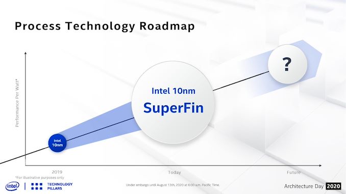
However, I now have an official decoder ring for you, to act as a reference for both users and Intel’s own engineers alike.
j4QW4rm.png


Does anyone really think that the original 10nm was anything but a complete disaster? Perhaps the article would help change minds of some of these skeptics.
 
Back
Top