Report an Error


NVIDIA GT200B
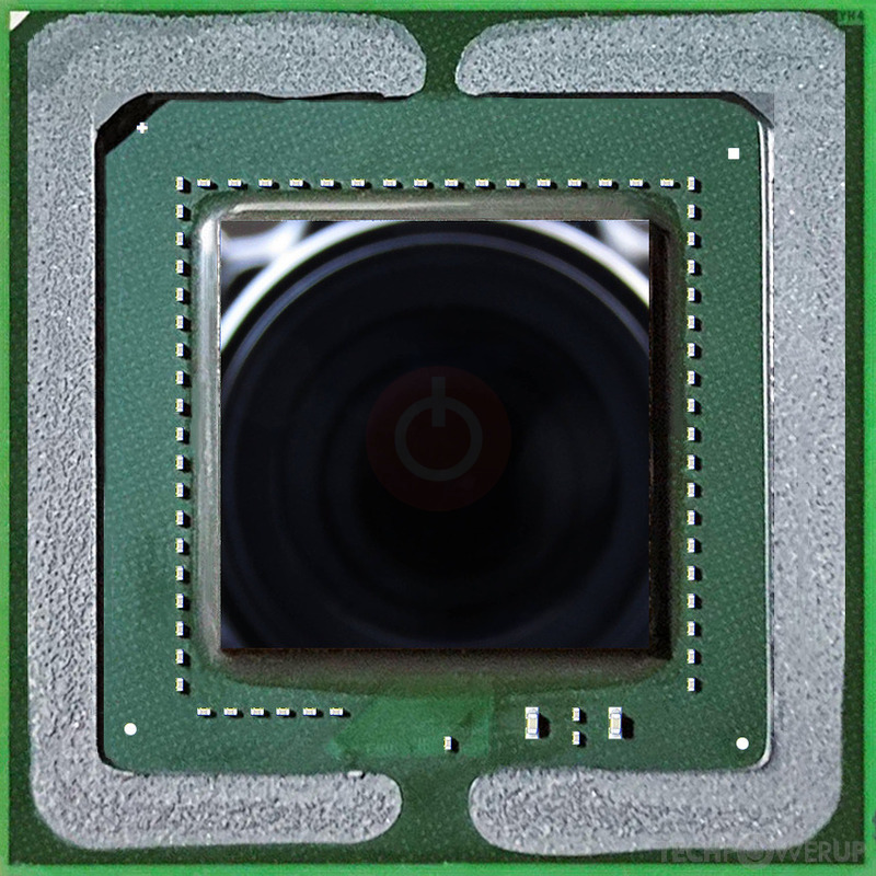
GT200B

Heat Spreader

G200-105-B3

G200-350-B3

G200-400-B3
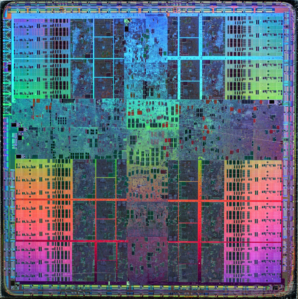
Fritzchens Fritz
Die Shot

Die TPC
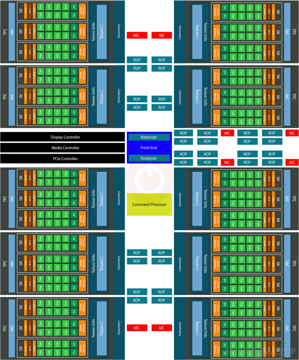
Block Diagram

TPC Diagram
NVIDIA's GT200B GPU uses the Tesla 2.0 architecture and is made using a 55 nm production process at TSMC. With a die size of 470 mm² and a transistor count of 1,400 million it is a very big chip. GT200B supports DirectX 11.1 (Feature Level 10_0). For GPU compute applications, OpenCL version 1.1 and CUDA 1.3 can be used. It features 240 shading units, 80 texture mapping units and 32 ROPs.
Graphics Processor
- Released
- Jun 1st, 2008
- GPU Name
- GT200B
- Codename
- NVA0
- Architecture
- Tesla 2.0
- Foundry
- TSMC
- Process Size
- 55 nm
- Transistors
- 1,400 million
- Density
- 3.0M / mm²
- Die Size
- 470 mm²
- Package
- BGA-1981
Graphics Features
- DirectX
- 11.1 (10_0)
- OpenGL
- 3.3
- OpenCL
- 1.1
- Vulkan
- N/A
- CUDA
- 1.3
- Shader Model
- 4.0
- WDDM
- 1.2
- PureVideo HD
- VP2
- VDPAU
- Feature Set A
Render Config
- Shading Units
- 240
- TMUs
- 80
- ROPs
- 32
- SM Count
- 30
- SFUs
- 60
- TPCs
- 10
- Tex L1 Cache
- 24 KB per TPC
- L2 Cache
- 256 KB
- Max. TDP
- 800 W
All Tesla 2.0 GPUs
NVIDIA GPU Architecture History
- 2024 Blackwell
- 2023 Hopper
- 2022-2024 Ada Lovelace
- 2020-2024 Ampere
- 2018-2022 Turing
- 2017-2020 Volta
- 2016-2021 Pascal
- 2014-2019 Maxwell 2.0
- 2014-2017 Maxwell
- 2013-2015 Kepler 2.0
- 2012-2018 Kepler
- 2010-2016 Fermi 2.0
- 2010-2013 VLIW Vec4
- 2010-2016 Fermi
- 2007-2013 Tesla 2.0
- 2006-2010 Tesla
- 2003-2013 Curie
- 2003-2005 Rankine
- 2001-2003 Kelvin
- 1999-2005 Celsius
- 1998-2000 Fahrenheit
Graphics cards using the NVIDIA GT200B GPU
| Name | Chip | Memory | Shaders | TMUs | ROPs | GPU Clock | Memory Clock |
|---|---|---|---|---|---|---|---|
| G200-350-B3 | 1024 MB | 240 | 80 | 32 | 648 MHz | 1242 MHz | |
| G200-400-B3 | 896 MB | 240 | 80 | 28 | 576 MHz | 999 MHz | |
| G200-103-B2 | 896 MB | 216 | 72 | 28 | 576 MHz | 999 MHz | |
| G200-105-B3 | 896 MB | 240 | 80 | 28 | 633 MHz | 1134 MHz | |
| G200-350-B3 | 1024 MB | 240 | 80 | 32 | 648 MHz | 1242 MHz | |
| 4 GB | 240 | 80 | 32 | 648 MHz | 800 MHz | ||
| 4 GB | 240 | 80 | 32 | 648 MHz | 800 MHz | ||
| 4 GB | 240 | 80 | 32 | 610 MHz | 800 MHz | ||
| 1536 MB | 192 | 64 | 24 | 602 MHz | 800 MHz | ||
| G200-835-B2 | 1024 MB | 192 | 64 | 16 | 600 MHz | 800 MHz | |
| 1536 MB | 192 | 64 | 24 | 602 MHz | 800 MHz | ||
| 1536 MB | 192 | 64 | 24 | 602 MHz | 800 MHz | ||
| 1024 MB | 240 | 80 | 32 | 610 MHz | 800 MHz | ||
| 4 GB | 240 | 80 | 32 | 610 MHz | 800 MHz | ||
| 4 GB | 240 | 80 | 32 | 610 MHz | 800 MHz | ||
| 2 GB | 240 | 80 | 32 | 610 MHz | 800 MHz | ||
| G200-105-B3 | 896 MB | 240 | 80 | 28 | 633 MHz | 1134 MHz | |
| 4 GB | 240 | 80 | 32 | 610 MHz | 800 MHz | ||
| G200-103-B3 | 896 MB | 192 | 64 | 28 | 576 MHz | 999 MHz | |
| G200-350-B3 | 2 GB | 240 | 80 | 32 | 648 MHz | 1152 MHz | |
| G200-400-B3 | 896 MB | 240 | 80 | 28 | 576 MHz | 1008 MHz |


GT200B GPU Notes
| PureVideo HD: VP2 VDPAU: Feature Set A GT200B, commonly printed on the chip package as G200-xxx-Bx is an optical shrink of the G200 core to the newer 55 manufacturing process of TSMC. It helped shrink the core's energy and thermal footprints to a level that even facilitated building a dual-GPU accelerator |
May 7th, 2024 00:55 EDT
change timezone
Latest GPU Drivers
New Forum Posts
- Intel Core "Special Edition" Owners' Club (27)
- Overheating/undervolt/setup issues (9)
- Gigabyte Aorus Elite AX V2 rev 1.1 BIOS update "AMD AGESA V2 1.2.0.B" (6)
- Only some humans can see refresh rates faster than others, I am one of those humans. (203)
- The Official Thermal Interface Material thread (1169)
- What's your latest tech purchase? (20450)
- GPU Hot Spot Temperature 105 Celsius, fans at 3000 RPM, while GPU Temperature is max 70 Celsius (40)
- Cybersecurity - OSINT Software for Linux (3)
- nvflashk - Flash any BIOS to NVIDIA GPUs - Safe board ID bypass up to 4xxx series (241)
- RTX 2070 8GB unable to flash (0)
Popular Reviews
- Finalmouse UltralightX Review
- Cougar Hotrod Royal Gaming Chair Review
- Meze Audio LIRIC 2nd Generation Closed-Back Headphones Review
- Corsair iCUE Link RX120 RGB 120 mm Fan Review
- Upcoming Hardware Launches 2023 (Updated Feb 2024)
- ASRock NUC BOX-155H (Intel Core Ultra 7 155H) Review
- AMD Ryzen 7 7800X3D Review - The Best Gaming CPU
- ASUS Radeon RX 7900 GRE TUF OC Review
- Montech Sky Two GX Review
- HYTE THICC Q60 240 mm AIO Review
Controversial News Posts
- Intel Statement on Stability Issues: "Motherboard Makers to Blame" (248)
- Windows 11 Now Officially Adware as Microsoft Embeds Ads in the Start Menu (167)
- AMD to Redesign Ray Tracing Hardware on RDNA 4 (166)
- Sony PlayStation 5 Pro Specifications Confirmed, Console Arrives Before Holidays (118)
- AMD's RDNA 4 GPUs Could Stick with 18 Gbps GDDR6 Memory (114)
- NVIDIA to Only Launch the Flagship GeForce RTX 5090 in 2024, Rest of the Series in 2025 (108)
- NVIDIA Points Intel Raptor Lake CPU Users to Get Help from Intel Amid System Instability Issues (106)
- AMD Ryzen 9 7900X3D Now at a Mouth-watering $329 (104)