Report an Error


NVIDIA GeForce GTX 275
- Graphics Processor
- GT200B
- Cores
- 240
- TMUs
- 80
- ROPs
- 28
- Memory Size
- 896 MB
- Memory Type
- GDDR3
- Bus Width
- 448 bit


GPU

PCB Front
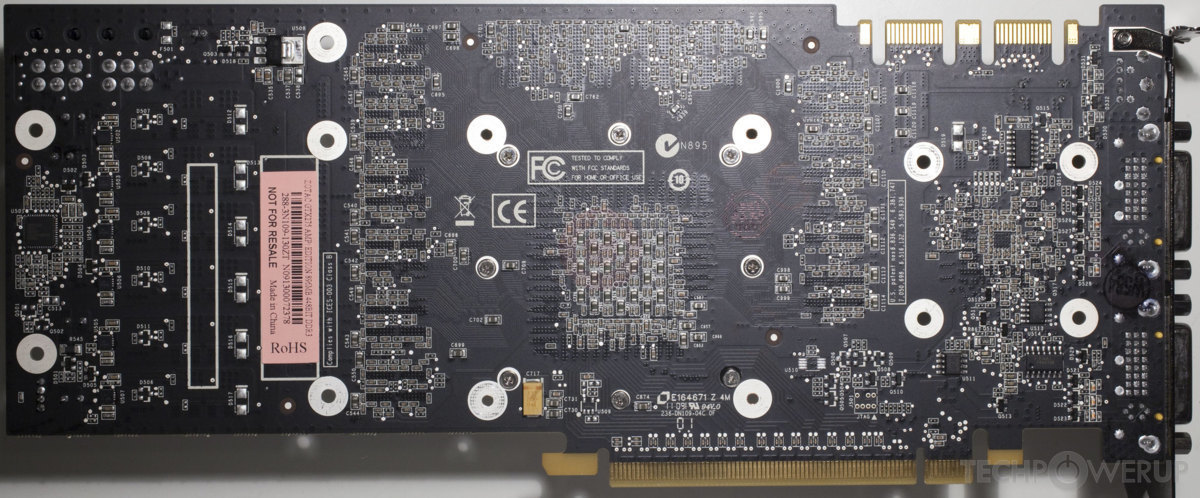
PCB Back
Recommended Gaming Resolutions:
- 1366x768
- 1600x900
- 1920x1080
The GeForce GTX 275 was a performance-segment graphics card by NVIDIA, launched on January 15th, 2009. Built on the 55 nm process, and based on the GT200B graphics processor, in its G200-105-B3 variant, the card supports DirectX 11.1. Even though it supports DirectX 11, the feature level is only 10_0, which can be problematic with many DirectX 11 & DirectX 12 titles. The GT200B graphics processor is a large chip with a die area of 470 mm² and 1,400 million transistors. It features 240 shading units, 80 texture mapping units, and 28 ROPs. NVIDIA has paired 896 MB GDDR3 memory with the GeForce GTX 275, which are connected using a 448-bit memory interface. The GPU is operating at a frequency of 633 MHz, memory is running at 1134 MHz.
Being a dual-slot card, the NVIDIA GeForce GTX 275 draws power from 2x 6-pin power connectors, with power draw rated at 219 W maximum. Display outputs include: 2x DVI. GeForce GTX 275 is connected to the rest of the system using a PCI-Express 2.0 x16 interface. The card measures 267 mm in length, and features a dual-slot cooling solution. Its price at launch was 249 US Dollars.
Being a dual-slot card, the NVIDIA GeForce GTX 275 draws power from 2x 6-pin power connectors, with power draw rated at 219 W maximum. Display outputs include: 2x DVI. GeForce GTX 275 is connected to the rest of the system using a PCI-Express 2.0 x16 interface. The card measures 267 mm in length, and features a dual-slot cooling solution. Its price at launch was 249 US Dollars.
Graphics Processor
Graphics Card
- Release Date
- Jan 15th, 2009
- Generation
- GeForce 200
- Predecessor
- GeForce 9
- Successor
- GeForce 400
- Production
- End-of-life
- Launch Price
- 249 USD
- Bus Interface
- PCIe 2.0 x16
- Reviews
- 61 in our database
Relative Performance
Based on TPU review data: "Performance Summary" at 1920x1080, 4K for 2080 Ti and faster.
Clock Speeds
- GPU Clock
- 633 MHz
- Shader Clock
- 1404 MHz
- Memory Clock
-
1134 MHz
2.3 Gbps effective
Memory
- Memory Size
- 896 MB
- Memory Type
- GDDR3
- Memory Bus
- 448 bit
- Bandwidth
- 127.0 GB/s
Render Config
- Shading Units
- 240
- TMUs
- 80
- ROPs
- 28
- SM Count
- 30
- L2 Cache
- 224 KB
Theoretical Performance
- Pixel Rate
- 17.72 GPixel/s
- Texture Rate
- 50.64 GTexel/s
- FP32 (float)
- 673.9 GFLOPS
- FP64 (double)
- 84.24 GFLOPS (1:8)
Board Design
- Slot Width
- Dual-slot
- Length
- 267 mm
10.5 inches
- TDP
- 219 W
- Suggested PSU
- 550 W
- Outputs
- 2x DVI
- Power Connectors
- 2x 6-pin
- Board Number
- P897 SKU 54
Graphics Features
- DirectX
- 11.1 (10_0)
- OpenGL
- 3.3
- OpenCL
- 1.1
- Vulkan
- N/A
- CUDA
- 1.3
- Shader Model
- 4.0
GT200B GPU Notes
| PureVideo HD: VP2 VDPAU: Feature Set A GT200B, commonly printed on the chip package as G200-xxx-Bx is an optical shrink of the G200 core to the newer 55 manufacturing process of TSMC. It helped shrink the core's energy and thermal footprints to a level that even facilitated building a dual-GPU accelerator |
Retail boards based on this design (5)
| Name | GPU Clock | Memory Clock | Other Changes |
|---|---|---|---|
| 648 MHz | 1185 MHz | 270 mm/10.6 inches, 1x DVI 1x HDMI 1x VGA | |
| 715 MHz | 1260 MHz | 1792 MB, 1x DVI 1x mini-HDMI 1x VGA | |
| 700 MHz | 1150 MHz | 1792 MB, 270 mm/10.6 inches, 1x DVI 1x HDMI 1x VGA | |
| 666 MHz | 1161 MHz | 2x DVI 1x S-Video | |
| 702 MHz | 1260 MHz | 2x DVI 1x S-Video |


Apr 25th, 2024 23:40 EDT
change timezone
Latest GPU Drivers
New Forum Posts
- Alphacool CORE 1 CPU block - bulging with danger of splitting? (18)
- What's your latest tech purchase? (20340)
- Black screen after muting (5)
- What phone you use as your daily driver? And, a discussion of them. (1481)
- What are you playing? (20530)
- Secure boot already open help (0)
- TPU's Nostalgic Hardware Club (18465)
- Post your Speedometer 3.0 Score (36)
- Size on Disk Excessively Different than Size (9)
- Dell Workstation Owners Club (3056)
Popular Reviews
- Fractal Design Terra Review
- Thermalright Phantom Spirit 120 EVO Review
- Corsair 2000D Airflow Review
- ASUS GeForce RTX 4090 STRIX OC Review
- NVIDIA GeForce RTX 4090 Founders Edition Review - Impressive Performance
- ASUS GeForce RTX 4090 Matrix Platinum Review - The RTX 4090 Ti
- MSI GeForce RTX 4090 Suprim X Review
- Gigabyte GeForce RTX 4090 Gaming OC Review
- MSI GeForce RTX 4090 Gaming X Trio Review
- MSI GeForce RTX 4090 Suprim Liquid X Review
Controversial News Posts
- Sony PlayStation 5 Pro Specifications Confirmed, Console Arrives Before Holidays (117)
- Windows 11 Now Officially Adware as Microsoft Embeds Ads in the Start Menu (110)
- NVIDIA Points Intel Raptor Lake CPU Users to Get Help from Intel Amid System Instability Issues (106)
- AMD "Strix Halo" Zen 5 Mobile Processor Pictured: Chiplet-based, Uses 256-bit LPDDR5X (101)
- US Government Wants Nuclear Plants to Offload AI Data Center Expansion (98)
- AMD's RDNA 4 GPUs Could Stick with 18 Gbps GDDR6 Memory (88)
- Developers of Outpost Infinity Siege Recommend Underclocking i9-13900K and i9-14900K for Stability on Machines with RTX 4090 (85)
- Windows 10 Security Updates to Cost $61 After 2025, $427 by 2028 (84)