Report an Error


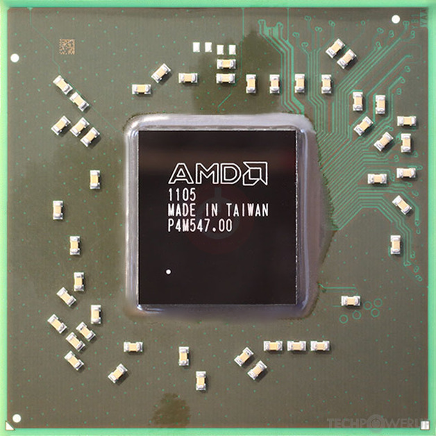
Acer HD 6750M
- Graphics Processor
- Whistler
- Cores
- 480
- TMUs
- 24
- ROPs
- 8
- Memory Size
- 1024 MB
- Memory Type
- GDDR5
- Bus Width
- 128 bit

GPU
Graphics Processor
- GPU Name
- Whistler
- GPU Variant
-
Whistler PRO
(216-0810005)
- Architecture
- TeraScale 2
- Foundry
- TSMC
- Process Size
- 40 nm
- Transistors
- 716 million
- Density
- 6.1M / mm²
- Die Size
- 118 mm²
- Chip Package
- FCBGA-962/1336
Mobile Graphics
Clock Speeds
- GPU Clock
- 600 MHz
- Memory Clock
-
800 MHz
1600 Mbps effective
3.2 Gbps effective
Memory
- Memory Size
- 1024 MB
- Memory Type
GDDR3
GDDR5
- Memory Bus
- 128 bit
- Bandwidth
-
25.60 GB/s
51.20 GB/s
Render Config
- Shading Units
- 480
- TMUs
- 24
- ROPs
- 8
- Compute Units
- 6
- L1 Cache
- 8 KB (per CU)
- L2 Cache
- 256 KB
Theoretical Performance
- Pixel Rate
- 4.800 GPixel/s
- Texture Rate
- 14.40 GTexel/s
- FP32 (float)
- 576.0 GFLOPS
Board Design
- Slot Width
- MXM Module
- TDP
- 35 W
- Outputs
- Portable Device Dependent
Graphics Features
- DirectX
- 11.2 (11_0)
- OpenGL
- 4.4
- OpenCL
- 1.2
- Vulkan
- N/A
- Shader Model
- 5.0
Whistler GPU Notes
| Generation: Northern Islands Desktop Variant: Turks Mobile Variant: Thames Graphics/Compute: GFX4 Display Core Engine: 5.0 Unified Video Decoder: 3.1 |
Other retail boards based on this design (2)
| Name | GPU Clock | Memory Clock | Other Changes |
|---|---|---|---|
|
Acer HD 6750M

|
600 MHz | 800 MHz | GDDR5 |
| 598 MHz | 794 MHz | 512 MB, GDDR5 |

May 10th, 2024 04:01 EDT
change timezone
Latest GPU Drivers
New Forum Posts
- Is hard drive sentinel trustworthy (8)
- RM750x (2021) enough for my 5800X3D + 7900XT system? (0)
- Ghost of Tsushima PC Port !!!! (23)
- Flash VBIOS to turn RX 580 2048SP into RX 570 (28)
- AM5 boot times improve RADICALLY with memory context restore enabled (28)
- looking to optimize (performance+cooling) a ryzen 7800x3d system with x670e aorus pro x (16)
- Any suggestion for hosting to test something ? (4)
- Last game you purchased? (279)
- The TPU UK Clubhouse (24791)
- RTX40x0 VBIOS viewer: Kepler-Ada NVIDIA VBIOS Visualizer - opensource pattern for ImHex (0)
Popular Reviews
- CHERRY XTRFY M64 Pro Review
- Bykski CPU-XPR-C-I CPU Water Block Review - Amazing Value!
- Corsair iCUE Link RX120 RGB 120 mm Fan Review
- Corsair MP700 Pro SE 4 TB Review
- ThundeRobot ML903 NearLink Review
- Upcoming Hardware Launches 2023 (Updated Feb 2024)
- Finalmouse UltralightX Review
- AMD Ryzen 7 7800X3D Review - The Best Gaming CPU
- Sapphire Radeon RX 7700 XT Pure Review
- ASUS Radeon RX 7900 GRE TUF OC Review
Controversial News Posts
- Intel Statement on Stability Issues: "Motherboard Makers to Blame" (264)
- AMD to Redesign Ray Tracing Hardware on RDNA 4 (206)
- Windows 11 Now Officially Adware as Microsoft Embeds Ads in the Start Menu (169)
- NVIDIA to Only Launch the Flagship GeForce RTX 5090 in 2024, Rest of the Series in 2025 (144)
- Sony PlayStation 5 Pro Specifications Confirmed, Console Arrives Before Holidays (119)
- AMD's RDNA 4 GPUs Could Stick with 18 Gbps GDDR6 Memory (114)
- NVIDIA Points Intel Raptor Lake CPU Users to Get Help from Intel Amid System Instability Issues (106)
- AMD Ryzen 9 7900X3D Now at a Mouth-watering $329 (104)