Report an Error


AMD Radeon HD 7650M
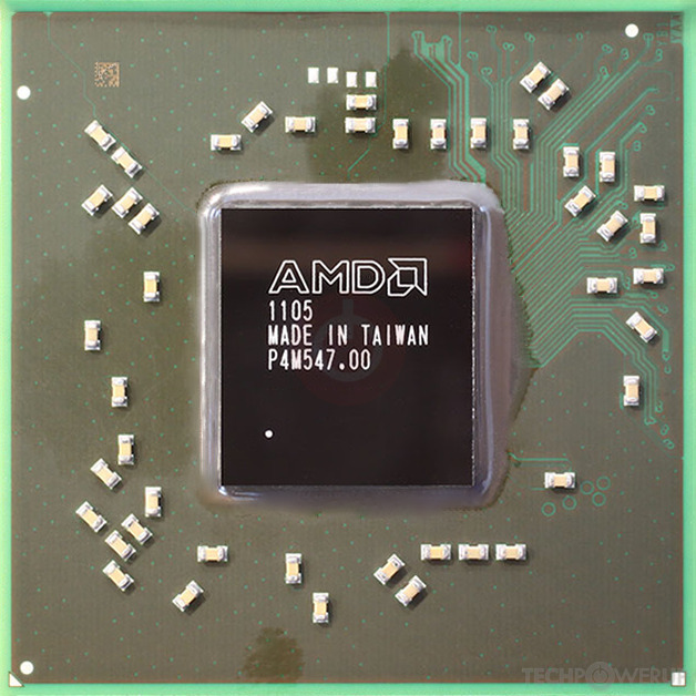
- Graphics Processor
- Thames
- Cores
- 480
- TMUs
- 24
- ROPs
- 16
- Memory Size
- 1024 MB
- Memory Type
- DDR3
- Bus Width
- 128 bit

GPU
Graphics Processor
- GPU Name
- Thames
- GPU Variant
-
Thames M2 PRO
(216-0833002)
- Architecture
- TeraScale 2
- Foundry
- TSMC
- Process Size
- 40 nm
- Transistors
- 716 million
- Density
- 6.1M / mm²
- Die Size
- 118 mm²
- Chip Package
- FCBGA-631/962
Mobile Graphics
- Release Date
- Jan 7th, 2012
- Generation
-
London
(HD 7600M)
- Predecessor
- Vancouver
- Successor
- Solar System
- Production
- End-of-life
- Bus Interface
- PCIe 2.0 x16
Clock Speeds
- GPU Clock
500 MHz
550 MHz (+10%)
- Memory Clock
-
800 MHz
1600 Mbps effective
Memory
- Memory Size
- 1024 MB
- Memory Type
- DDR3
- Memory Bus
- 128 bit
- Bandwidth
- 25.60 GB/s
Render Config
- Shading Units
- 480
- TMUs
- 24
- ROPs
- 16
- Compute Units
- 6
- L1 Cache
- 8 KB (per CU)
- L2 Cache
- 256 KB
Theoretical Performance
- Pixel Rate
-
8.000 GPixel/s
8.800 GPixel/s
- Texture Rate
-
12.00 GTexel/s
13.20 GTexel/s
- FP32 (float)
-
480.0 GFLOPS
528.0 GFLOPS
Board Design
- TDP
- 20 W
- Outputs
- Portable Device Dependent
Graphics Features
- DirectX
- 11.2 (11_0)
- OpenGL
- 4.4
- OpenCL
- 1.2
- Vulkan
- N/A
- Shader Model
- 5.0
Card Notes
| Memory Variant: 2048MB DDR3 Memory Variant: 1024MB GDDR3 Memory Variant: 2048MB GDDR3 |
Thames GPU Notes
| Generation: Northern Islands Desktop Variant: Turks Mobile Variant: Whistler Graphics/Compute: GFX4 Display Core Engine: 5.0 Unified Video Decoder: 3.1 |
Other retail boards based on this design (2)
| Name | GPU Clock | Memory Clock | Other Changes |
|---|---|---|---|
|
AMD Radeon HD 7650M

|
550 MHz | 800 MHz | |
| 500 MHz | 900 MHz | 2 GB, HyperMemory |

Apr 26th, 2024 22:54 EDT
change timezone
Latest GPU Drivers
New Forum Posts
- Black screens leading to restarts (Event ID 18) on AMD platform since changing graphics card (43)
- FINAL FANTASY XIV: Dawntrail Official Benchmark (73)
- Your PC ATM (34509)
- Rare GPUs / Unreleased GPUs (1877)
- looking to build a new system and im considering asrock brand but i have some doubts/concerns. (15)
- AAF Optimus DCH Audio Modded Driver for Windows 10/11 - For ALL HDAUDIO Enumerator Chips (652)
- Help me identify rx 580 card ? (0)
- Strange system crashes out of nowhere help (9)
- What phone you use as your daily driver? And, a discussion of them. (1494)
- Secure boot already open help (11)
Popular Reviews
- Ugreen NASync DXP4800 Plus Review
- HYTE THICC Q60 240 mm AIO Review
- Quick Look: MOONDROP CHU 2 Budget In-Ear Monitors
- MOONDROP x Crinacle DUSK In-Ear Monitors Review - The Last 5%
- Thermalright Phantom Spirit 120 EVO Review
- Upcoming Hardware Launches 2023 (Updated Feb 2024)
- Alienware Pro Wireless Gaming Keyboard Review
- CeBIT 2008: Akasa Review
- FiiO K19 Desktop DAC/Headphone Amplifier Review
- CeBIT 2008: Cyber E Sport Review
Controversial News Posts
- Windows 11 Now Officially Adware as Microsoft Embeds Ads in the Start Menu (135)
- Sony PlayStation 5 Pro Specifications Confirmed, Console Arrives Before Holidays (117)
- NVIDIA Points Intel Raptor Lake CPU Users to Get Help from Intel Amid System Instability Issues (106)
- AMD "Strix Halo" Zen 5 Mobile Processor Pictured: Chiplet-based, Uses 256-bit LPDDR5X (103)
- US Government Wants Nuclear Plants to Offload AI Data Center Expansion (98)
- AMD's RDNA 4 GPUs Could Stick with 18 Gbps GDDR6 Memory (95)
- Developers of Outpost Infinity Siege Recommend Underclocking i9-13900K and i9-14900K for Stability on Machines with RTX 4090 (85)
- Windows 10 Security Updates to Cost $61 After 2025, $427 by 2028 (84)