Report an Error


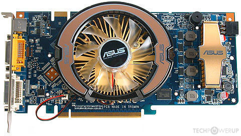
ASUS 8800 GS TOP
- EN8800GS-TOP/HTDP/384M
- Graphics Processor
- G92
- Cores
- 96
- TMUs
- 48
- ROPs
- 12
- Memory Size
- 384 MB
- Memory Type
- GDDR3
- Bus Width
- 192 bit

GPU
Graphics Processor
Graphics Card
- Release Date
- Jan 31st, 2008
- Generation
-
GeForce 8
(8800)
- Predecessor
- GeForce 7 PCIe
- Successor
- GeForce 9
- Production
- End-of-life
- Bus Interface
- PCIe 2.0 x16
Clock Speeds
- GPU Clock
550 MHz
600 MHz (+9%)
- Shader Clock
1375 MHz
1700 MHz (+24%)
- Memory Clock
-
800 MHz
900 MHz (+13%)
1600 Mbps effective
1800 Mbps effective
Memory
- Memory Size
- 384 MB
- Memory Type
- GDDR3
- Memory Bus
- 192 bit
- Bandwidth
-
38.40 GB/s
43.20 GB/s
Render Config
- Shading Units
- 96
- TMUs
- 48
- ROPs
- 12
- SM Count
- 12
- L2 Cache
- 48 KB
Theoretical Performance
- Pixel Rate
-
6.600 GPixel/s
7.200 GPixel/s
- Texture Rate
-
26.40 GTexel/s
28.80 GTexel/s
- FP32 (float)
-
264.0 GFLOPS
326.4 GFLOPS
Board Design
- Slot Width
- Single-slot
- TDP
- 105 W
- Suggested PSU
- 300 W
- Outputs
- 2x DVI
1x S-Video
- Power Connectors
- 1x 6-pin
- Board Number
- P393 SKU 4
Graphics Features
- DirectX
- 11.1 (10_0)
- OpenGL
- 3.3
- OpenCL
- 1.1
- Vulkan
- N/A
- CUDA
- 1.1
- Shader Model
- 4.0
Card Notes
| Memory Variant: 768 MB |
G92 GPU Notes
| PureVideo HD: VP2 VDPAU: Feature Set A |
Other retail boards based on this design (1)
| Name | GPU Clock | Memory Clock | Other Changes |
|---|---|---|---|
|
ASUS 8800 GS TOP

|
600 MHz | 900 MHz |
May 9th, 2024 19:38 EDT
change timezone
Latest GPU Drivers
New Forum Posts
- My Arc A310 doesm't display upon boot somewhat (1)
- GTX 1650 Bios disappears after installing driver (2)
- What's your latest tech purchase? (20489)
- Your way of cooling your PC? (97)
- looking to optimize (performance+cooling) a ryzen 7800x3d system with x670e aorus pro x (14)
- Last game you purchased? (278)
- AM5 boot times improve RADICALLY with memory context restore enabled (15)
- Keysfan (25)
- Microsoft butchering Xbox Studios (41)
- Flash VBIOS to turn RX 580 2048SP into RX 570 (25)
Popular Reviews
- CHERRY XTRFY M64 Pro Review
- Corsair iCUE Link RX120 RGB 120 mm Fan Review
- Bykski CPU-XPR-C-I CPU Water Block Review - Amazing Value!
- Finalmouse UltralightX Review
- Upcoming Hardware Launches 2023 (Updated Feb 2024)
- Corsair MP700 Pro SE 4 TB Review
- AMD Ryzen 7 7800X3D Review - The Best Gaming CPU
- Cougar Hotrod Royal Gaming Chair Review
- ASUS Radeon RX 7900 GRE TUF OC Review
- Meze Audio LIRIC 2nd Generation Closed-Back Headphones Review
Controversial News Posts
- Intel Statement on Stability Issues: "Motherboard Makers to Blame" (264)
- AMD to Redesign Ray Tracing Hardware on RDNA 4 (206)
- Windows 11 Now Officially Adware as Microsoft Embeds Ads in the Start Menu (169)
- NVIDIA to Only Launch the Flagship GeForce RTX 5090 in 2024, Rest of the Series in 2025 (144)
- Sony PlayStation 5 Pro Specifications Confirmed, Console Arrives Before Holidays (119)
- AMD's RDNA 4 GPUs Could Stick with 18 Gbps GDDR6 Memory (114)
- NVIDIA Points Intel Raptor Lake CPU Users to Get Help from Intel Amid System Instability Issues (106)
- AMD Ryzen 9 7900X3D Now at a Mouth-watering $329 (104)