Report an Error


Sapphire HD 3450 AGP
- 11160-01
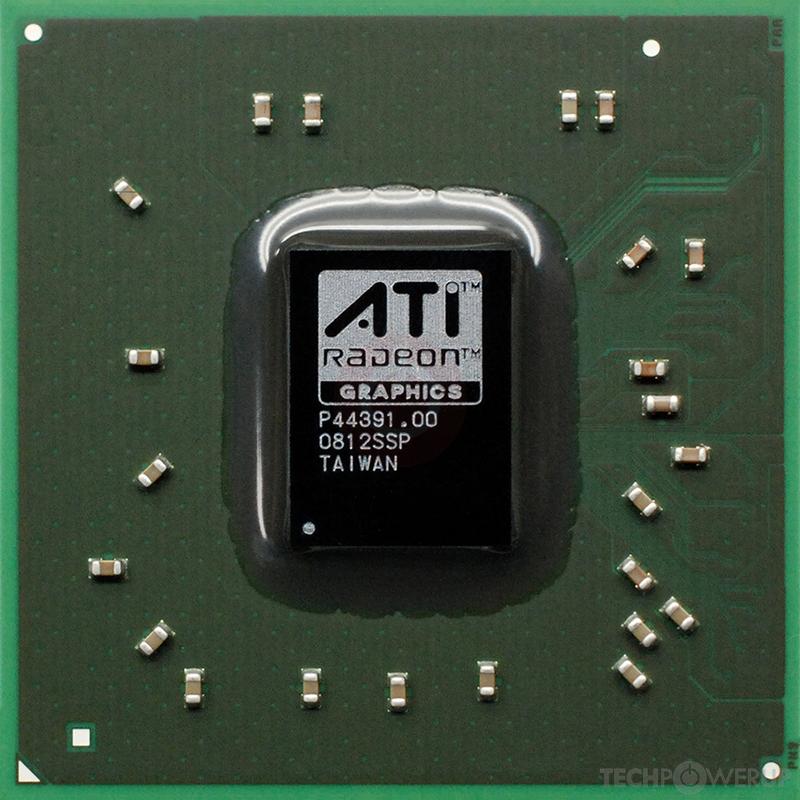
- Graphics Processor
- RV620
- Cores
- 40
- TMUs
- 4
- ROPs
- 4
- Memory Size
- 512 MB
- Memory Type
- DDR2
- Bus Width
- 64 bit

GPU
Graphics Processor
Graphics Card
- Release Date
- Jan 23rd, 2008
- Generation
-
Radeon R600
(HD 3400)
- Predecessor
- Radeon R500 PCIe
- Successor
- Radeon R700
- Production
- End-of-life
- Bus Interface
- AGP 8x
Clock Speeds
- GPU Clock
- 600 MHz
- Memory Clock
-
500 MHz
400 MHz (-20%)
1000 Mbps effective
800 Mbps effective
Memory
- Memory Size
- 512 MB
- Memory Type
- DDR2
- Memory Bus
- 64 bit
- Bandwidth
-
8.000 GB/s
6.400 GB/s
Render Config
- Shading Units
- 40
- TMUs
- 4
- ROPs
- 4
- Compute Units
- 2
- L2 Cache
- 64 KB
Theoretical Performance
- Pixel Rate
- 2.400 GPixel/s
- Texture Rate
- 2.400 GTexel/s
- FP32 (float)
- 48.00 GFLOPS
Board Design
- Slot Width
- Single-slot
- TDP
- 25 W
- Suggested PSU
- 200 W
- Outputs
2x DVI
1x DVI
1x HDMI
1x VGA
- Power Connectors
1x Molex
Floppy
Graphics Features
- DirectX
- 10.1 (10_1)
- OpenGL
- 3.3
- OpenCL
- N/A
- Vulkan
- N/A
- Shader Model
- 4.1
RV620 GPU Notes
| Mobile Variant: M82 / M84 Codename: Koopa Graphics/Compute: GFX3 Display Core Engine: 3.0 Unified Video Decoder: 1.0 |
Other retail boards based on this design (1)
| Name | GPU Clock | Memory Clock | Other Changes |
|---|---|---|---|
|
Sapphire HD 3450 AGP

|
600 MHz | 400 MHz | 1x DVI 1x HDMI 1x VGA |
Apr 27th, 2024 00:51 EDT
change timezone
Latest GPU Drivers
New Forum Posts
- Strange system crashes out of nowhere, help (13)
- RX 580 VBIOS related functionality not supported for Device: 0x67df (9)
- Alphacool CORE 1 CPU block - bulging with danger of splitting? (33)
- hacked (78)
- 5800x (and other Zen 3 chips) PBO settings/Temperature fix (937)
- Is this a hardware problem ? Live kernel 193 (0)
- Help me to OC my 5700X (11)
- Realtek Modded Audio Driver for Windows 10/11 - Only for HDAUDIO (5690)
- What's your latest tech purchase? (20355)
- AAF Optimus DCH Audio Modded Driver for Windows 10/11 - For ALL HDAUDIO Enumerator Chips (654)
Popular Reviews
- Ugreen NASync DXP4800 Plus Review
- HYTE THICC Q60 240 mm AIO Review
- MOONDROP x Crinacle DUSK In-Ear Monitors Review - The Last 5%
- Upcoming Hardware Launches 2023 (Updated Feb 2024)
- Quick Look: MOONDROP CHU 2 Budget In-Ear Monitors
- Thermalright Phantom Spirit 120 EVO Review
- FiiO K19 Desktop DAC/Headphone Amplifier Review
- Alienware Pro Wireless Gaming Keyboard Review
- AMD Ryzen 7 7800X3D Review - The Best Gaming CPU
- Corsair iCUE Link XC7 RGB Elite CPU Water Block Review
Controversial News Posts
- Windows 11 Now Officially Adware as Microsoft Embeds Ads in the Start Menu (135)
- Sony PlayStation 5 Pro Specifications Confirmed, Console Arrives Before Holidays (117)
- NVIDIA Points Intel Raptor Lake CPU Users to Get Help from Intel Amid System Instability Issues (106)
- AMD "Strix Halo" Zen 5 Mobile Processor Pictured: Chiplet-based, Uses 256-bit LPDDR5X (103)
- US Government Wants Nuclear Plants to Offload AI Data Center Expansion (98)
- AMD's RDNA 4 GPUs Could Stick with 18 Gbps GDDR6 Memory (95)
- Developers of Outpost Infinity Siege Recommend Underclocking i9-13900K and i9-14900K for Stability on Machines with RTX 4090 (85)
- Windows 10 Security Updates to Cost $61 After 2025, $427 by 2028 (84)