News Posts matching #28nm

Return to Keyword Browsing

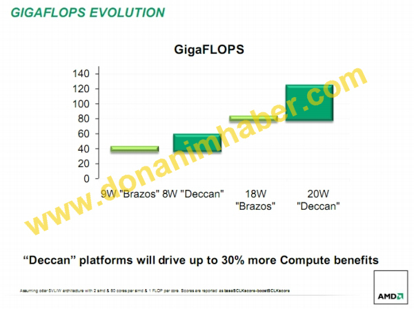
Fujitsu and SuVolta Demo ULV Operation of SRAM Down to ~0.4V

Fujitsu Semiconductor Limited and SuVolta, Inc. today announced that they have successfully demonstrated ultra-low-voltage operation of SRAM (static random access memory) blocks down to 0.425V by integrating SuVolta's PowerShrink low-power CMOS platform into Fujitsu Semiconductor's low-power process technology. By reducing power consumption, these technologies will make possible the ultimate in "ecological" products in the near future. Technology details and results will be presented at the 2011 International Electron Devices Meeting (IEDM) being held in Washington DC, starting December 5th.

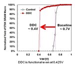
Controlling power consumption is the primary limiter of adding features to product types ranging from mobile electronics to tethered servers and networking equipment. The biggest contributor to power consumption is supply voltage. Previously, the power supply voltage of CMOS steadily reduced to approximately 1.0V at the 130nm technology node, but it has not reduced much further as technology has scaled to the 28nm node. To reduce the power supply voltage, one of the biggest obstacles is the minimum operating voltage of embedded SRAM blocks.

Are Improving Integrated Graphics Slowly Killing Off Discrete Graphics Cards?

Intel started the trend of improving integrated graphics with their second generation LGA1155 socket Core i3, i5 & i7 line of processors. Depending on the model, these processors sport integrated HD2000 or HD3000 graphics right on the processor die, which nowadays give acceptable performance for low-end gaming and can play Full HD 1080p video perfectly. This trend is increasing with the upcoming Ivy Bridge processors, which will be able to support a massive 4096 x 4096 pixel display, as we reported here. AMD now also have equivalent products with their Llano-based A-series processors. So, where does this leave discrete graphics cards? Well, the low end market is certainly seeing reduced sales, as there really isn't enough of a performance difference nowadays to always warrant an upgrade from an IGP. As integrated graphics improve further, one can see how this will hurt sales of higher end graphics cards too. The problem is that the bulk of the profit comes not from the top-end powerhouse graphics cards, but from the low to mid-end cards which allow these companies to remain in business, so cannibalizing sales of these products to integrated graphics could make high-end graphics cards a much more niche product and crucially, much more expensive with to boot.

TSMC 28 nm Technology in Volume Production

TSMC today announced that its 28nm process is in volume production and production wafers have been shipped to customers. TSMC leads the foundry segment to achieve volume production at 28nm node.

TSMC's 28nm process offering includes 28nm High Performance (28HP), 28nm High Performance Low Power (28HPL), 28nm Low Power (28LP), and 28nm High Performance Mobile Computing (28HPM). Among these technology offerings, 28HP, 28HPL and 28LP are all in volume production and 28HPM will be ready for production by the end of this year. The production-version design collateral of 28HPM has been distributed to most mobile computing customers for their product-design use.

AMD Showcases its First 28 nm GPU

AMD showed off its first graphics processor (GPU) built on TSMC's cutting-edge 28 nanometer silicon fabrication process, the next foundry process standard for discrete GPUs. Bulk manufacturing at TSMC's Fab 15 facility at 28 nm is still taking shape, TSMC will take volume orders only later this year. For the moment, it can run small batches for designers to test their designs. The GPU was running on a mobile platform (pictured below, the red PCB), cooled by a compact copper-channel air cooler, leading us to believe that this is a mainstream segment GPU, if not lower. The demo platform was showcased running DirectX 11 title Dirt 3. Besides that, absolutely no other details were shared, not even a company codename for the GPU board.

AMD's Next-Generation Wichita and Krishna APUs Detailed

In its latest presentation to industry partners, AMD detailed its upcoming Deccan low-power computing platform, targeting the market Intel's Atom and VIA's Nano processors do. AMD is currently behind the "Zacate" and "Ontario" processors, which deliver high performance/watt x86 computing at low power draw and costs. The company's future platform will be called "Deccan," consisting of processors codenamed "Wichita" and "Krishna," targeting the ULV desktop and netbook markets, respectively. With the next generation, AMD is looking to take advantage of the 28 nanometer manufacturing process to put four x86-64 cores based on the Bobcat architecture on a single piece of silicon, with an integrated memory controller and AMD Radeon discrete-class graphics.

The biggest change here isn't the fact that there are four cores, or that it's built on 28 nm, but that Wichita and Krishna are completely single-chip. The FCH or Fusion Controller Hub has been completely fused into the APU silicon. Motherboards and notebook logic boards will have just one big chip, with no "chipset" of any form. This makes AMD's Wichita and Krishna the industry's very first true x86-based consumer SoC (system on chip). The integrated memory controller now supports DDR3-1600 MHz memory. The integrated AMD Radeon graphics is set to get a performance and SIMD boost, as well, including a Secure Asset Management Unit (SAMU). AMD's next generation APUs are slated for 2012.

GLOBALFOUNDRIES Fabs in New York and Dresden Achieve Ready for Equipment Milestone

Just over one year after revealing plans for a major global capacity expansion, GLOBALFOUNDRIES today announced its newly constructed cleanrooms in New York and Dresden are ready for the installation of 300mm semiconductor wafer fabrication equipment. Achieving "Ready for Equipment" (RFE) status marks the transition from the construction phase to the operations phase-a significant milestone on the path to volume manufacturing in these new facilities.

"At GLOBALFOUNDRIES, we continue to invest aggressively in driving sustained growth on advanced technologies," said GLOBALFOUNDRIES CEO Ajit Manocha. "The build-out of our 300mm manufacturing campuses in New York and Dresden is supporting growing customer demand for advanced technologies, while creating hundreds of jobs and providing a significant boost to the economies in the surrounding regions. By completing these massive construction projects on schedule and on budget, we are continuing to deliver on our commitment to being the only truly global foundry."

Foundry Delays to Push Back NVIDIA Kepler Launch to 2012

It looks like foundry issues are back to slow down the launch of NVIDIA's next generation high-end GPU, codenamed Kepler. The delay may push Kepler's launch to 2012, it was expected to launch by late 2011. The 28 nanometer silicon fabrication process at TSMC, a principal foundry partner of NVIDIA, is producing unsatisfactory yields. Add to that, Kepler's performance is lower than expected.

TSMC's 28 nm process at Fab 15 facility has already seen delays, which have even shaped AMD's designs in a big way. AMD had originally planned to design high-end VLIW4 chips on the 32 nm process at TSMC, but later decided to wait for the 28 nm process, leading to plans of 32 nm GPUs being scrapped by both GPU designers. TSMC was supposed to be in a position take orders of high-end 28 nm GPUs by Q4 2011, and was set to start pilot production for its 20nm process technology in the third quarter of 2012.

TSMC Reiterates 28 nm Readiness by Q4 2011

TSMC reiterated that it will be ready with a 28 nanometer manufacturing process by Q4 2011. The semiconductor company handles manufacturing of graphics processors for both AMD and NVIDIA. After the current 40 nm process, 32 nm, the next milestone process, was canceled for GPU makers to leap to 28 nm, this caused the foundry transition to the next process to take longer than usual. The current 40 nm process already seems to be saturated by GPUs with over 3 billion transistors, which are barely able to maintain acceptable thermal specs without using some sort of power-load throttling mechanism.

TSMC Chairman and CEO, Morris Chang, confirmed that tape-outs will be starting as early as in Q3, and production of 28 nm chips will start in Q4. Chang expects that up to 3% of TSMC's revenues will be made from 28 nm chips by the end of the year. "We plan to have around 2% or 3% of our total revenue in the fourth quarter [to] be 28nm. The tape-outs of the 28-nanaometer will start to ramp in the second half, starting in the third quarter and then more in the fourth quarter. But the real momentum [for 28nm], we believe, will be next year," Chang said. Apart from GPUs, the 28 nm process will also benefit ARM processors, with multi-core ARM chips clocked at 3 GHz being on cards. The 28 nm bulk process will also dish out AMD's next generation accelerated processing units (APUs).

ARM and TSMC Sign Long-Term Strategic Agreement

ARM and Taiwan Semiconductor Manufacturing Company, Ltd. (TWSE: 2330, NYSE: TSM) today jointly announced a long-term agreement that provides TSMC with access to a broad range of ARM processors and enables the development of ARM physical IP across TSMC technology nodes. This agreement supports the companies' mutual customers to achieve optimized Systems-On-Chip (SoC) based on ARM processors and covers a wide range of process nodes extending down to 20nm.

The agreement provides TSMC access to optimize the implementation of ARM processors on TSMC process technologies, including ARM Cortex processor family and CoreLink interconnect fabric for AMBA protocols. It also establishes a long-term relationship with ARM for the development of physical IP, including memory products and standard cell libraries targeting the most advanced TSMC 28nm and 20nm processes.

TSMC Begins Construction on Gigafab in Central Taiwan

TSMC today held a groundbreaking ceremony in Taichung's Central Taiwan Science Park for Fab 15, TSMC's third 12-inch (300mm) Gigafab and an important milestone in the company's pledge to expand investment in Taiwan.

The groundbreaking ceremony was conducted by TSMC Chairman and CEO Dr. Morris Chang. "Science Parks have played a critical role in the development of Taiwan's high-tech industry. They have also provided important support to TSMC as we grew to become a leading global semiconductor company with its roots in Taiwan," Dr. Chang said. "Over the past two decades, TSMC has flourished in the Hsinchu and Tainan science parks, and our groundbreaking for Fab 15 today sets the foundation for TSMC to reach new heights."

GLOBALFOUNDRIES and ARM Define the Standard for Mobile Technology Platform Innovation

At the 2010 Mobile World Congress, GLOBALFOUNDRIES and ARM today unveiled new details on their leading-edge System-on-Chip (SoC) platform technology for powering the next generation of wireless products and applications. The new chip manufacturing platform is projected to enable a 40 percent increase in computing performance, a 30 percent decrease in power consumption, and a 100 percent increase in standby battery life. The new platform includes collaboration on two GLOBALFOUNDRIES process variants: 28nm super low power (SLP) for mobile and consumer applications and 28nm high performance (HP) for applications requiring maximum performance.

"The success of the next generation of mobile products will be increasingly dependent on their ability to deliver PC-class performance, a highly integrated rich media experience and longer battery life," said GLOBALFOUNDRIES chief operating officer Chia Song Hwee. "These demands are going to require a strong technology foundation and close collaboration between industry leaders to enable an increasing number of design companies to unlock this innovation. We are working closely with ARM to optimize the physical IP and implementation of the Cortex-A9 processor with our proven manufacturing experience in high-volume, advanced technology products, to deliver a fully integrated platform for leading-edge wireless products and applications."

ARM and GLOBALFOUNDRIES Partner to Build ARM SoC Products on 28 nm HKMG Process

ARM and GLOBALFOUNDRIES today announces a long-term strategic relationship to provide their mutual customers with an innovative SoC enablement program. To support the long-term relationship, GLOBALFOUNDRIES and ARM have signed a broad agreement on processor implementation and circuit optimization to provide mutual customers with a robust enablement program geared towards next-generation applications.

The SoC enablement program, built around a full suite of ARM Physical IP, Fabric IP and Processor IP, will deliver customers unparalleled design flexibility on GLOBALFOUNDRIES' most advanced HKMG semiconductor manufacturing capabilities. The collaborative efforts of the partnership will initially focus on enabling SoC products which use the low power and high performance ARM Cortex -A9 processor on GLOBALFOUNDRIES 28nm HKMG process. The characteristics of GLOBALFOUNDRIES 28nm "Gate First" HKMG technology is optimized for high performance processing with minimal leakage making it an ideal choice for advanced mobile solutions.

GLOBALFOUNDRIES To Highlight 32nm/28nm Technology Leadership at GSA Expo

As the semiconductor industry begins its transition to the next technology node, GLOBALFOUNDRIES is on track to take its position as the foundry technology leader. On October 1 at the Global Semiconductor Alliance Emerging Opportunities Expo & Conference in Santa Clara, Calif., GLOBALFOUNDRIES (Booth 321) will provide the latest details on its technology roadmap for the 32nm/28nm generations and its innovative "Gate First" approach to building transistors based on High-K Metal Gate (HKMG) technology.

"With each new technology generation, semiconductor foundries are increasingly challenged with the economics to sustain R&D and the know-how to bring these technologies to market in high-volume," said Len Jelinek, director and chief analyst, iSuppli. "With a heritage of rapidly ramping leading-edge technologies to high volumes at mature yields, combined with aggressive investments in capacity and technology, GLOBALFOUNDRIES is uniquely-positioned to challenge for next-generation foundry leadership."

TSMC Achieves 28 nm SRAM Yield Breakthrough

Taiwan Semiconductor Manufacturing Company, Ltd. has become the first foundry not only to achieve 28 nm functional 64 Mb SRAM yield, but also to achieve it across all three 28 nm nodes.

"Achieving 64 Mb SRAM yield across all three 28 nm process nodes is striking. It is particularly noteworthy because this achievement demonstrates the manufacturing benefits of the gate-last approach that we developed for the two TSMC 28 nm high-k metal gate processes," explained Dr. Jack Sun, vice president, Research and Development at TSMC.

"This accomplishment underscores TSMC's process technology capability and value in 28 nm. It shows TSMC is not only able to extend conventional SiON technology to 28 nm, but is also able to deliver the right 28 nm HKMG technology at the same time," explained Dr. Mark Liu, senior vice president, Advanced Technology Business at TSMC.

IBM Announces Availability of 28 nm Semiconductor Technology

In a move that signals a firm and ongoing commitment to advanced semiconductor technology leadership, IBM, Chartered Semiconductor Manufacturing Ltd., GLOBALFOUNDRIES, Infineon Technologies, Samsung Electronics, Co., Ltd., and STMicroelectronics have defined and are jointly developing a 28-nanometer, high-k metal gate (HKMG), low-power bulk complementary metal oxide semiconductor (CMOS) process technology.

The low-power, 28nm technology platform can provide power-performance and time-to-market advantages for producers of a broad range of power-sensitive mobile and consumer electronics applications, including the fast-growing mobile Internet device market segment. The favorable leakage characteristics of the HKMG technology result in optimized battery life for the next generation of mobile products.
Return to Keyword Browsing
Apr 26th, 2024 06:03 EDT change timezone

New Forum Posts

Popular Reviews

Controversial News Posts