News Posts matching #32 nm

Return to Keyword Browsing

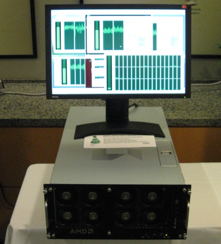
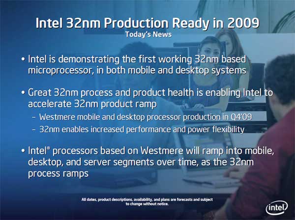
Intel Commences 32 nm Chip Production

Intel's foundries have commenced mass production of the company's first processors based on the 32 nm second generation high-K metal gate (HKMG) technologies. With these the company's next-generation Westmere architecture becomes retail-grade. The first products will include dual-core processors compatible with the recently introduced socket LGA-1156 platforms, and will carry the brand identifiers (and model number schemes) Core i5 600 series, Core i3 500 series, and Pentium dual-core series.

The desktop-grade parts are based on the "Clarkdale" core, and notebook-grade ones "Arrandale". The latter will be introduced first among the two, with the first Arrandale chips slated for Q4 2009, while the desktop chips arrive a little later in Q1 2010. Intel will focus on this transition to the Westmere architecture in the upcoming Intel Developer Forum event.

Westmere a Fast 'Tick'?

Intel has already set foot on the 32 nm lithography, with first 32 nm based prcoessors expected to arrive in Q1 2010. These processors have already been extensively sampled, and tested by sections of the media. More importantly, 32 nm marks Intel's introduction of the Westmere architecture, which is a 32 nm optical shrink of Nehalem, with a slightly expanded feature-set making use of the possibly higher transistor loads. Starting with dual-core "Clarkale" processor, Intel plans to work out high-end six-core processors codenamed "Gulftown" within the first half of 2010. In addition to this, Intel is readying Westmere's successor, codenamed "Sandy Bridge".

While a vague die-shot of a supposedly mainstream quad-core processor based on Sandy Bridge surfaced last month, more information about it is coming to light from industry sources, according to DigiTimes. Intel will introduce the Sandy Bridge architecture in the fourth quarter of 2010. Considering the first Westmere CPUs are commercially launched ten months after its formal introduction (Westmere was unveiled in February,) the commercial launch of the first Sandy Bridge processors can't be too far away from Q4 2010. This in essence shows that Intel can afford to come up with a new flavour of CPUs every year. Nehalem will have served as a 1.25 year "tock" for the 45 nm process, while Westmere may serve as a "tick" of nearly the same length. For those of you unfamiliar with Intel's "tick-tock" model of product development cycle, The company uses a "tick-tock" model of process development, where each processor architecture gets to be made in two manufacturing processes, while each process gets to build two succeeding architectures.

Intel Clarksfield Mobile Quad-Core Chips Feature Low TDPs

Using new lows in core clock speeds, Intel is looking to give its upcoming Westmere-based Core i7 "Clarksfield" mobile quad-core processors surprisingly low rated TDPs. Apart from the rest of the known lineup of upcoming Intel processors, it is learned that Intel will initially have three mobile quad-core chips, all branded Core i7, and based on the 32 nm Clarksfield core. The three will include an Extreme Edition (XE) SKU. The clock speeds of these will be surprisingly low: ranged between 1.60 to 2.00 GHz, while having a high Turbo-Boost speed ranged between 2.80 to 3.20 GHz.

The Turbo-Boost speed is enabled when the processor powers-down some of its cores, and increases the clock speed of the cores that are available. In the process, power consumption is reduced. These chips have some very low TDPs that make them ideal for notebooks. The XE variant has a TDP of 55W, while the two lower models have rated TDP of 45W. The low-end model comes with 6 MB of L3 cache, while the higher two have 8 MB. All models have four cores with HyperThreading enabling 8 threads, and lack IGPs. They will run on the new PGA-G1 socket.

In related news, the first three Core i5/i7 "Lynnfield" processors come with rated TDP no higher than 95W. They come with Turbo-Boost Speeds ranging between 3.20 and 3.60 GHz.

Intel SandyBridge Mainstream Quad-Core CPU Architecture Surfaces

Intel is on a golden path, showing no signs of a slowdown as far as technology development is concerned. After having pushed its 32 nm manufacturing node and its derived Westmere architecture to production grade, Intel seems to have already made a prototype on the 32 nm node, which will serve a technology leap on 32 nm. The company uses a "tick-tock" model of process development, where each processor architecture gets to be made in two manufacturing processes, while each process gets to build two succeeding architectures. The current Nehalem architecture meets 32 nm with the Westmere architecture, while the 32 nm node meets its next architecture with the SandyBridge.

SandyBridge is characterised by a larger level of integration of components. While Nehalem and Westmere "Lynnfield" and "Clarksfield" mainstream processors use a multi-chip module that holds the CPU and north-bridge dice, SandyBridge will see an integration of both into a monolithic, rectangular die spreading across an area of around 225 sq. mm. Significant portions of the die will be occupied with a DirectX 11-compliant integrated graphics processor, the "SandyBridge System Agent" (a component which includes a PCI-Express hub, and DMI. The L3 cache is the largest component on the die. It will have a large 256-bit ring-topology, which lets it not only perform cache operations, but also as a fast transport medium between the various components.

Intel 32 nm Clarkdale Chip Brought Forward to Q4 2009

While the bulk of Intel's upcoming Nehalem and Westmere derived products include quad-core processors, the company hasn't left out dual-core processors just as yet. The dual-core Core i5 desktop processor will be based on the new Clarkdale core, built on the 32 nm Westmere architecture. Originally slated for a Q1 2010 launch, the new chip seems to have been pulled into the Q4 2009 launch schedule, deep enough to make for a significant amount of projected sales, according to sources in the Taiwanese motherboard industry.

The sales projections for Q4 look particularly interesting. Core i5 "Clarkdale" dual-core is projected to amount for 10% of Intel's sales, while Core i7 "Bloomfield" at 1%, Core i5 "Lynnfield" at 2% (Core i7 "Lynnfield" is slated for Q1 2010), Core 2 Quad at 9%, Core 2 Duo E7000/E8000 at 35%, Pentium E5000/E6000 at 31%, Celeron E3000 and Atom together at 9%, Pentium E2000 and Celeron 400 together at 4%. In the following quarter, Clarkdale's sales share is expected to rise to 20%. The numbers prove just how large the market for dual-core processors is, even four years into the introduction of quad-core chips.

Intel Delays Launch of Core i5 Platform

Intel's Core i5 series marks the consumer mainstream entry of the Nehalem architecture, in a bid to propagate quad-core processors, at the same time letting the market digest existing inventories of dual-core processors, and making sure its foundries are well-oiled to cater to the 32 nm process, Intel is giving its "Lynnfield" quad-core processor a quarter's head-start. Taiwanese industry observer DigiTimes notes that the platform' debut may have been delayed by a little over a month.

Originally slated for July, the industry debut of Lynnfield and its launch companion, Intel P55 chipset, have been pushed to early September. Stocks of the processors and compatible motherboards however, will be in time for the launch. The processors may be available to retailers about a week ahead, in late August itself, while compatible motherboards even earlier, in mid-August.

Intel plans to start the lineup with three models (yet to be named), clocked at 2.66 GHz, 2.80 GHz, and 2.93 GHz, and priced at US $194, $284, and $562 respectively (in 1000-unit tray quantities). Major motherboard vendors such as ASUS, Gigabyte, and MSI have already displayed some of their first compatible motherboards. The P55 chipset itself is expected to be priced at $40.

At Least 30% of NVIDIA GPU Shipments on TSMC 40 nm Process by End of 2009

Nearly a month since AMD's introduction of the 40 nm RV740 GPU, there is still no concrete sign of a 40 nm GPU from NVIDIA slated for anytime soon, apart from timely scoops on the GT300. Sources at graphics card vendors however seem confident that by the end of 2009, 40 nm GPUs will constitute at least 30% of NVIDIA's GPU shipments, that too sourced from TSMC, a foundry-partner which has been in the news off late, for technical problems with their 40 nm node, that are affecting its output efficiency.

What's more, NVIDIA seems to have expressed interest in becoming one of the first clients for TSMC's upcoming 28 nm process that is expected to become a reality in Q1 2010. This should also tell you that for GPUs, the next step for silicon fabrication technology will be 28 nm, unlike 32 nm for CPUs.

Toshiba to Launch World's First 32 nm Process NAND Flash Memory

Toshiba Corporation, reinforcing its leadership in the development and fabrication of cutting-edge, high density NAND flash memory, today announced that it will start shipping NAND flash memory products fabricated with 32nm process technology. Samples of the world's first 32 nm generation, 32-gigabit (Gb) single chips (4 gigabytes (GB)), offering the largest density of any NAND flash chip, are available from today, and 16 Gb chip (2 GB) products, the current mainstream density, will be available in July in Japan. The 32 Gb chips will first be applied to memory cards and USB memories and subsequently extended to embedded products.

AMD Demos 48-core Opteron Server

Having recently made its plans with the server market public, AMD demonstrated a 4-socket server featuring four 12-core, next-generation Opteron processors. That's 48 cores in all. The company has pulled its six-core Istanbul Opteron processors' launch from H2 2008 to Q2 2008, and is set to launch its Opteron 6000 series processors based on the "Magny Cours" architecture in 2010.

Processors in the series come with 8 or 12 cores. The company seems to be ready with a few of these, enough to put together a 4-socket demo system. While AMD did not run any benchmarks on the system, it managed to draw some attention due to the fact that there hasn't been so much parallelism in a 4-way server till date. On the course of its 2010 launch, the company may hold more demonstrations, perhaps with benchmarks to show how the platform compares to competing solutions from rival Intel. The "Magny Cours" processor will be the first in line for the company's G34 "Maranello" platform for AMD Opteron 6000 series processors with up to 16 cores, 4 sockets, and quad-channel memory interfaces per socket. The 16-core processor in the making is slated for 2011, is based on the Bulldozer architecture, and will be built on the 32 nm process.

Core i5 Specifications and Prices Surface

Intel's next big thing in the making, the Core i5 series processors are nearing launch, which is reportedly delayed to October. The new processors replace the Core 2 Quad and Core 2 Duo series of processors, while leaving the high-end market for Core i7 to play with. These processors are based on the LGA 1156 socket, and are incompatible with Core i7 motherboards. Recent reports shed light on three models in the making to start the lineup, all of which are quad-core processors based on the Lynnfield core, built on the existing 45 nm process.

The common features of these processors include: four x86 processing cores with support for HyperThreading technology, an integrated dual-channel DDR3 memory controller specified to run DDR3-1066 and DDR3-1333 modules, 8 MB of L3 cache, and support for TurboBoost technology. The three models will come with core clock speeds of 2.66 GHz, 2.80 GHz, and 2.93 GHz. The three will be priced at US $196, $284, and $562 respectively. With the TurboBoost technology enabled, the clock speeds card be stepped up to 3.2, 3.46 and 3.6 GHz respectively, on the fly. Shortly after launching these processors, Intel may introduce the industry's first 32 nm processors. With these prices, the chips clearly intrude the price-domain of Core i7, though perhaps their lower platform costs could serve as deal-makers.

Photos Emerge of Intel's 32 nm Clarkdale Processor

Not long after Intel was said to have sent out samples of its new 32 nm mainstream processor based on Nehalem micro-architecture, someone over at XS forums, has posted photos of an as yet unnamed Clarkdale processor, running at 2.4 GHz, with 4 MB L3 Cache. The only official information from Intel we have about these processors is what we covered two months ago, when Intel spread open its plans to deal with the mainstream and value markets using its Nehalem micro-architecture.

Intel Displays Larrabee Wafer at IDF Beijing

Earlier this week, Intel conducted the Intel Developer Forum (IDF): Spring 2009 event at Beijing, China. Among several presentations on the the architectural advancements of the company's products, that include Nehalem and its scalable platforms, perhaps the most interesting was a brief talk by Pat Gelsinger, Senior Vice President and General Manager of Intel's Digital Enterprise Group, on Larrabee. The term is Intel's first "many cores" architecture used to work as a graphics processor. The architecture will be thoroughly backed by low-level and high-level programming languages and tools by Intel.

French website Hardware.fr took a timely snap off a webcast of the event, showing Gelsinger holding a 300 mm wafer of Larrabee dice. The theory that Intel has working prototypes of the GPU deep inside its labs gains weight. Making use of current-generation manufacturing technologies, Intel is scaling the performance of x86 processing elements, all 32+ of them. As you can faintly see from the wafer, Larrabee has a large die. It is reported that first generation of Larrabee will be built on the 45 nm manufacturing process. Products based on the architecture may arrive by late 2009, or early 2010. With the company kicking off its 32 nm production later this year, Larrabee may be built on the newer process a little later.

AMD 32 nm CPU Conquest to Begin in 2010

After spinning off its manufacturing division to The Foundry Co., AMD is left with all the engineering resources it needs to make processors. Contradicting older roadmap slides by the company predicting it would start selling 32 nm processors in 2011, Dirk Meyer, CEO of AMD in an interview with Information Week said that the company is on-track to ship smaller, more powerful processors built on the 32 nm manufacturing process by 2010.

The new manufacturing process would allow the chip maker to step up transistor counts to add more features and computational power. Tomorrow, on March 2, the AMD is expected to close the deal with Advanced Technology Investment Company (ATIC) of Abu Dhabi to form The Foundry Company (TFC). This would render AMD fabless. The company will then, like other fabless market heavyweights such as NVIDIA and VIA, will focus on designing processors, while TFC, its largest foundry partner will manufacture the processors. Currently AMD is tied up with foundry companies such as TSMC and UMC for manufacturing products of its Graphics Products Group, products such as GPUs and chipset.

AMD will be an year behind larger market rival Intel in selling processors built on the 32 nm technology. Intel plans to roll out 32 nm processors by Q4 2009. AMD's designs will be ready by mid-2010, following which volume production of its 32 nm chips will commence by Q4 2010.

Intel Presents 32 nm Westmere Family of Processors

Intel today spread opens its plans to deal with the mainstream and value markets using its Nehalem micro-architecture. The company introduced to the media and analysts, its plans concerning the upcoming Westmere family of processors, a term used to describe Intel processors built using the company's 32 nm second-generation high-K silicon fabrication technology, while being based on the Nehalem micro-architecture. The presentation demystifies all confusion surrounding the company canning plans of dual-core 45 nm Nehalem-derivatives. The presentation also sheds light on what approach Intel plans to adopt with bringing the new architecture to the enterprise segment.
Return to Keyword Browsing
May 12th, 2024 21:03 EDT change timezone

New Forum Posts

Popular Reviews

Controversial News Posts