News Posts matching #ASML

Return to Keyword Browsing

ASML's Ex-Employee in China Allegedly Stole Confidential Information

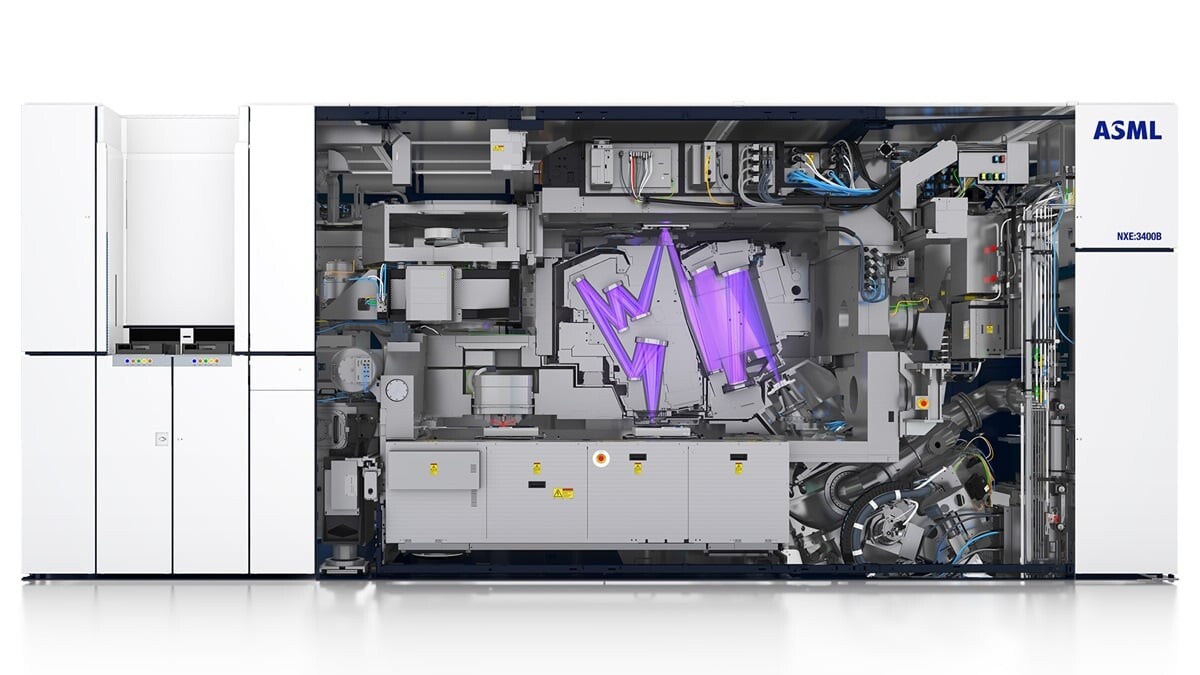
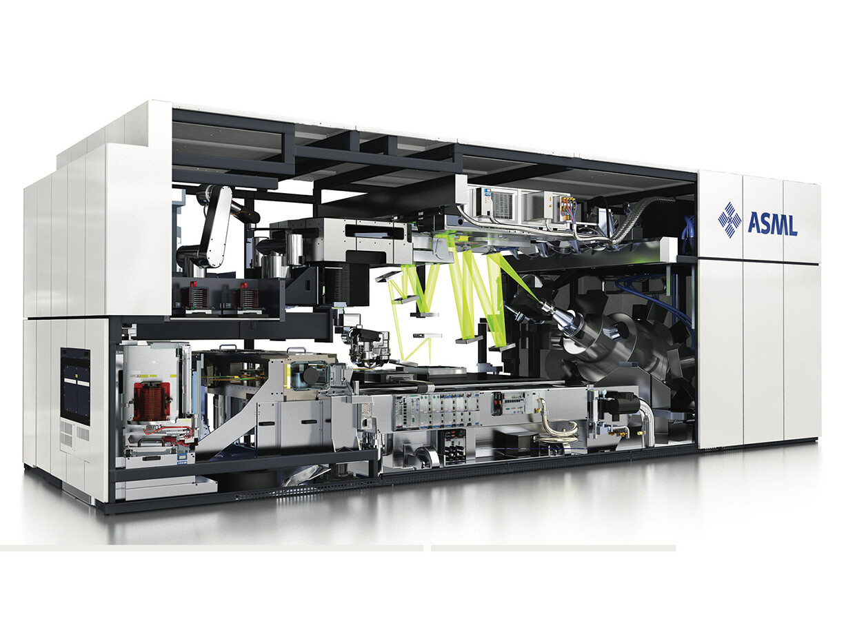
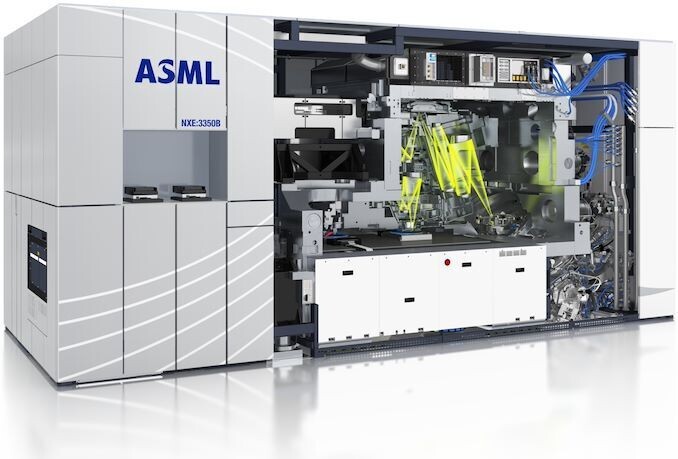
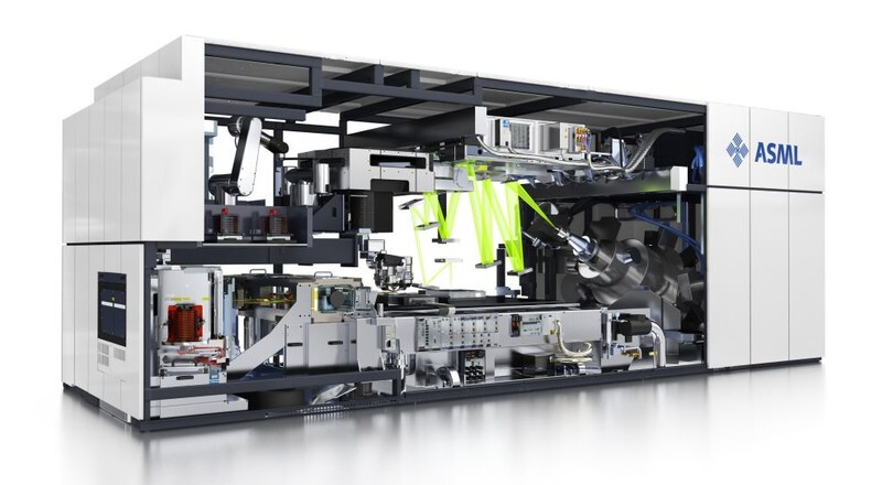
The Netherlands-based ASML has reportedly launched a comprehensive investigation into the company's branch in China following reports that one of its former employees allegedly stole confidential information. According to Bloomberg, the employee in question was part of a product life cycle management (PLM) program for ASML's advanced lithography solutions. Specifically, the employee worked for the Teamcenter software division responsible for lithography tool management. This software was used to create digital twins of scanners and other tools and allowed information to be shared among the company's employees. In ASML's case, the software contained all the confidential information about the scanners and how they work, which makes it a target for IP theft. We do not know if this is a China-sponsored action to boost its domestic lithography tool development; however, ASML has issued a statement below.
ASMLWe have experienced unauthorized misappropriation of data relating to proprietary technology by a (now) former employee in China. We promptly initiated a comprehensive internal review. Based upon our initial findings we do not believe that the misappropriation is material to our business. However, as a result of the security incident, certain export control regulations may have been violated. ASML has therefore reported the incident to relevant authorities. We are implementing additional remedial measures in light of this incident.

Japan and the Netherlands Said to Join US in Blocking Access to Chip Making Tools for China

According to Bloomberg, Japan and the Netherlands are getting ready to join the US in limiting access to advanced semiconductor manufacturing equipment for China. The three nations are currently in talks—that might end as soon as today—over how they can impose joint limits on what kind of equipment and tools can be exported to China. Apparently there will be no official announcement if a deal is struck, instead the restrictions will simply be implemented as required.

Bloomberg states that the Netherlands will expand export restrictions that ASML is already under, which according to the publication means stricter export rules around DEUV machines, which are used in cutting edge semiconductor nodes. Japan is said to implement similar export restrictions for Nikon as well as Tokyo Electron, with the US already having implemented restrictions for Applied Materials. The export restriction deal is in part being done to appease US equipment makers, who have complained that their international competitors haven't been under the same export restrictions when it comes to China, as they have. The question is if the export restrictions will hinder China in the long run, or if the nation will simply push ahead and develop its own, competing semiconductor manufacturing tools.

Update Jan 28th: Japan and the Netherlands reached an agreement with the US on Friday and the two countries are said to be making individual announcements with regards to their individual agreements with the US.

ASML Reports €21.2 Billion Net Sales and €5.6 Billion Net Income in 2022

Today ASML Holding NV (ASML) has published its 2022 fourth-quarter and full-year results. "Our fourth-quarter net sales came in around the midpoint of our guidance at €6.4 billion. The gross margin of 51.5% was above our guidance due to additional upgrades and insurance settlement for last year's ASML Berlin fire. "For ASML, 2022 was another strong year ending with total net sales for the year of €21.2 billion, gross margin of 50.5% and a record backlog at the end of 2022 of €40.4 billion.

"We continue to see uncertainty in the market caused by inflation, rising interest rates, risk of recession and geopolitical developments related to export controls. However, our customers indicate that they expect the market to rebound in the second half of the year. Considering our order lead times and the strategic nature of lithography investments, demand for our systems therefore remains strong.

TSMC Announces Updates for TSMC Arizona

TSMC today announced that in addition to TSMC Arizona's first fab, which is scheduled to begin production of N4 process technology in 2024, TSMC has also started the construction of a second fab which is scheduled to begin production of 3 nm process technology in 2026. The overall investment for these two fabs will be approximately US$40 billion, representing the largest foreign direct investment in Arizona history and one of the largest foreign direct investments in the history of the United States.

In addition to the over 10,000 construction workers who helped with construction of the site, TSMC Arizona's two fabs are expected to create an additional 10,000 high-paying high-tech jobs, including 4,500 direct TSMC jobs. When complete, TSMC Arizona's two fabs will manufacture over 600,000 wafers per year, with estimated end-product value of more than US $40 billion.

ASML Said to Have Plans to Bring European Supply Chain to Taiwan

Advanced Semiconductor Materials Lithography, or as the company is more commonly known, ASML, is apparently set to build a new factory in Taiwan for the production of advanced semiconductor lithography equipment. The new factory is said to be built in the Linkou area of New Taipei City and at the same time, bring with it its European supply chain, according to Taiwan Vice Premier Shen Jong-chin.

The new factory in Linkou is still some time away, as construction will only start in July, 2023. It will apparently be ASML's largest investment in Taiwan to date, although an exact figure of the investment wasn't given, but the new factory will take up 6.68 hectares or 66,800 square metres, suggesting it'll be a rather large facility. That said, not all the land will be used for the clean room facilities, as there will also be office buildings and warehouse buildings adjacent to the factory. No details on which suppliers ASML will bring with it to Taiwan, but it's likely that the likes of Zeiss, who supplies many of the mirrors in ASML's machines, will be setting up a local presence, alongside other key ASML suppliers. ASML already has an office in Hsinchu, about an hour south of New Taipei City.

ASML CTO Expects Post High-NA Lithography to be Prohibitively Costly

In an interview with Bits & Chips, ASML's CTO Martin van den Brink said that he believes that we might be reaching the end of the road for current semiconductor lithography technology in the not so distant future. However, for the time being, ASML is executing on its roadmap and after EUV, the next step is high-NA or high-numerical aperture and ASML is currently planning to have its first research high-NA scanner ready for a joint R&D venture with Imec in 2023. Assuming everything goes to plan, ASML is then planning on delivering the first R&D machines to its customers in 2024, followed by deliver of the first volume production machines using high-NA sometime in 2025. Van den Brink points out that due to the current supply chain uncertainties could affect the timing, in combination with the fact that ASML has a high demand for its EUV machines and the two technologies share a lot of components.

As such, current orders are the priority and high-NA development might be put on the back burner if need be, or as Van den Brink puts it "today's meal takes priority over tomorrow's." High-NA scanners are expected to be even more power hungry than EUV machines and are as such expected to pull around two Megawatts for the various stages. The next step in the evolution of semiconductor lithography is where ASML is expecting things to get problematic, as what the company is currently calling hyper-NA is expected to be prohibitively costly to manufacture and use. If the cost of hyper-NA grows as fast as we've seen in high-NA, it will pretty much be economically unfeasible," Van den Brink said. ASML is hoping to overcome the cost issues, but for now, the company has a plan for the next decade and things could very well change during that time and remove some of the obstacles that are currently being seen.

ASML Reports €5.4 Billion Net Sales and €1.4 Billion Net Income in Q2 2022

Today ASML Holding NV (ASML) has published its 2022 second-quarter results. Q2 net sales of €5.4 billion, gross margin of 49.1%, net income of €1.4 billion. Record quarterly net bookings in Q2 of €8.5 billion. ASML expects Q3 2022 net sales between €5.1 billion and €5.4 billion and a gross margin between 49% and 50%. Expected sales growth for the full year of around 10%.

The value of fast shipments*in 2022 leading to delayed revenue recognition into 2023 is expected to increase from around €1 billion to around €2.8 billion.
"Our second-quarter net sales came in at €5.4 billion with a gross margin of 49.1%. Demand from our customers remains very strong, as reflected by record net bookings in the second quarter of €8.5 billion, including €5.4 billion from 0.33 NA and 0.55 NA EUV systems as well as strong DUV bookings.

US Wants ASML to Stop Product Shipments to China

ASML is one of the critical semiconductors companies, as they provide tools for making actual silicon. Located in the Netherlands, they are famous for their DUV and EUV lithography tools, used to etch designs onto silicon wafers. According to the report from Bloomberg, the United States governing body is negotiating with the Dutch government to restrict the export of ASML's products to China. This came to affection following US Deputy Commerce Secretary Don Graves's visit to the Netherlands to discuss supply chain issues and meeting with ASML Chief Executive Officer Peter Wennink. While these suggested export restrictions could be beneficial to the strategic placement of US against China, it would hurt ASML's revenue as sales in China accounted for a 16% share of the company's revenue in 2021.

It is recorded that the Chinese spending spree on tools has been the greatest among every country, lasting for two years in a row. By banning ASML from exporting its lithography tools to China, the US could theoretically halt Chinese plans for achieving the government's intended semiconductor independence. The talks with the Dutch government and ASML are still a work in progress, so we are yet to see if the deal is finalized. Additionally, it is worth pointing out that the major US semiconductor manufacturing tool makers like Applied Materials and Lam Research are already banned from exporting to China.

ASML Reports Q1 2022 Financial Results

Our first-quarter net sales came in at €3.5 billion which is at the high end of our guidance. The gross margin of 49.0%, is as guided. Our first-quarter net bookings came in at €7.0 billion, including €2.5 billion from 0.33 NA and 0.55 NA EUV systems as well as very strong DUV bookings, reflecting the continued high demand for advanced and mature nodes.

"We continue to see that the demand for our systems is higher than our current production capacity. We accommodate our customers through offering high-productivity upgrades and reducing cycle time in our factories, and we continue to offer a fast shipment process. In addition, we are actively working to significantly expand capacity together with our supply chain partners. In light of the demand and our plans to increase capacity, we expect to revisit our scenarios for 2025 and growth opportunities beyond. We plan to communicate updates in the second half of the year.

Intel Installs First EUV Tool in Irish Fab 34

Last week Intel finalised the installation of its first EUV tool in Fab 34, which is located in Leixlip, Ireland. That comes just two months after Intel started installing its first chipmaking equipment in the fab. The EUV tool is made by ASML, but was shipped to Intel in Hillsboro, Oregon, USA first, before being sent back to Europe. It's unclear why it was shipped to the US first, but it's possible that Intel tested the equipment there and made sure it was to its spec, before shipping it to its new fab.

This is the first of several machines from ASML that are expected to be installed in Fab 34 and Intel says it's "a key enabler of Intel 4 process technology". The ASML machine required four unspecified Boeing aircrafts to ship, as well as 35 trucks to bring it to Fab 34. The machine, or tool as Intel calls it, has been sent in parts since December last year and has only now been completely assembled. For more details, see the video after the break.

ASML is the Next Bottle Neck in Chip Manufacturing

There have been several announcements of new semiconductor fabs being built all over the world, but those fabs might end up being empty shells, all because of a single company. ASML or Advanced Semiconductor Materials Lithography if you prefer, is a Dutch company that produces various types of photolithography machines that are used to produce semiconductors. They're the world leader in their field and their machines are used by the likes of Intel and TSMC to do the physical etching of the silicon wafers that semiconductors are produced from. Now a warning from ASML's CEO, Peter Wennink has arrived, stating that the company can't keep up with demand.

The company isn't expecting to fulfil orders for at least the next couple of years, despite expecting to ship more machines this year than last year and more machines next year than this year. As each of these machines are largely custom made for its customers and hand built, due to the low production volumes, it takes a lot of time to construct each of these huge machines. Wennink said that the company "really needs to step up our capacity significantly more than 50 per cent. That will take time."

Semiconductor Makers Don't Expect Russia-Ukraine War to Worsen Chip Shortages

Much of the globalized world's logistics is still in disarray from the COVID-19 pandemic, and now, Russia has thrown its weight on the matter through its invasion of Ukraine. As the initial offensive played out in the early hours of February 24th, semiconductor industry analysts turned to the situation with a prying eye - how exactly could this deadlock, and the following political and economical sanctions towards Russia, impact the semiconductor industry? The consensus seems to be a favorable one: not that much.

"The semiconductor industry has a diverse set of suppliers of key materials and gases, so we do not believe there are immediate supply disruption risks related to Russia and Ukraine," said John Neuffer, chief executive and president of the Semiconductor Industry Association. That sentiment was echoed by Intel; a company representative told Bloomberg that the company does not anticipate "(...) any impact on our supply chain. Our strategy of having a diverse, global supply chain minimizes our risk of potential local interruptions."

Intel Purchases ASML TWINSCAN EXE:5200 EUV Production System

Today, ASML Holding and Intel Corporation announced the latest phase of their longstanding collaboration to advance the cutting edge of semiconductor lithography technology. Intel has issued its first purchase order to ASML for the delivery of the industry's first TWINSCAN EXE:5200 system - an extreme ultraviolet (EUV) high-volume production system with a high numerical aperture and more than 200 wafers per hour productivity - as part of the two companies' long-term High-NA collaboration framework.

"Intel's vision and early commitment to ASML's High-NA EUV technology is proof of its relentless pursuit of Moore's Law. Compared to the current EUV systems, our innovative extended EUV roadmap delivers continued lithographic improvements at reduced complexity, cost, cycle time and energy that the chip industry needs to drive affordable scaling well into the next decade," said ASML President and CTO Martin van den Brink.

ASML Provides Damage Assessment of Fire Incident, EUV Component Production Affected

ASML, makers of vital semiconductor fabrication machinery powering the world's leading fabs, including TSMC, provided its first damage-assessment of the fire incident at one of its component plants near Berlin, on January 3. This plant manufactures several mechanical and optical components of semiconductor fabrication machinery, such as wafer tables and clamps, reticle chucks and mirror blocks.

ASML, in a press-release, disclosed that production of components used in DUV (deep-ultraviolet) machines, has been restarted, as that area of the plant is unaffected by the fire. A region of the plant that manufactures wafer clamps for use in its EUV (extreme ultraviolet) machines, however, has been affected by the fire. The company is still in the process of coming up with a recovery plan for this area, and will come up with a tentative date for restart of production only after that. EUV lithography is leveraged for 5 nm and upcoming 3 nm silicon fabrication nodes at TSMC, Samsung, and Intel. TSMC is known to be ASML's largest customer. ASML stated that it will release its Q4-2021 and full-year 2021 financial results on January 19, and it may provide more updates on the matter.
The press-release follows.

ASML, Makers of Semiconductor Fab Machinery, Reports a Fire Incident

ASML, the company that makes semiconductor fab machinery that powers most of today's cutting-edge foundries, has reported a fire incident in one of its plants near Berlin. The company reports that the incident occurred at night, none of its employees are injured, and that the fire is extinguished. The company says that it does not know at this point how the incident affects supplies, since it hasn't undertaken a damage-assessment. The Berlin plant of ASML manufactures components of silicon lithography equipment, including some key mechanical and optical components, such as wafer tables and clamps, reticle chucks and mirror blocks. ASML inherited this plant when it acquired Berliner Glas in 2020.

ASML Reports €5.2 Billion Net Sales and €1.7 Billion Net Income in Q3 2021

Today, ASML Holding NV (ASML) has published its 2021 third-quarter results. "Our third-quarter net sales came in at €5.2 billion with a gross margin of 51.7%, both within our guidance. Our third-quarter net bookings came in at €6.2 billion, including €2.9 billion from EUV systems. The demand continues to be high. The ongoing digital transformation and current chip shortage fuel the need to increase our capacity to meet the current and expected future demand for Memory and for all Logic nodes. ASML expects fourth-quarter net sales between €4.9 billion and €5.2 billion with a gross margin between 51% and 52%. ASML expects R&D costs of around €670 million and SG&A costs of around €195 million. For the full year, we are on track to achieving growth approaching 35%," said ASML President and Chief Executive Officer Peter Wennink.

Fabricating the Fabs: ASML Vision Document Predicts 300 Billion-Transistor Logic by 2030

"Moore's Law is alive and well," says ASML, in its vision document addressing investors. The company manufactures the machines that perform the actual task of silicon lithography—turning silicon discs into wafers of logic or storage chips. It highlighted the various technologies making progress, which will help its semiconductor-fabrication customers, such as TSMC and their hundreds of clients, sustain Moore's Law all the way through this decade. The company predicts SoCs with as many as 300 billion transistors by 2030. To achieve this, the company is innovating in two distinct directions—at the chip-level, to increase transistor density per chip to over 50 billion transistors; and at the system level, through packaging technology innovations, to reach that ultimate transistor count.

According to ASML's roadmap, at the turn of the decade, its technology enables 5 nm-class in production, and is at the cusp of a major breakthrough, nanosheet-FETs. which pave the way for 3 nm and 2 nm nodes, backed by EUV lithography. The journey from 2 nm to 1.5 nm will require another breakthrough, forked-nanosheets, and from 1.5 nm to 1 nm yet another breakthrough, CFET. Sub-1 nm fabrication will be possible toward the turn of this decade, thanks to 2D atomic channel technology, which is how chip-designers will be able to cram over 50 billion transistors per chip, and build MCM systems with over 300 billion transistors. The presentation predicts that besides 3D packaging, stacked silicon will also play a role, with multiple stacked logic layers, heterogenous chips with logic, storage, and I/O layers, stacked DRAM (up from single-digit layers to double-digits; and for NAND flash to grow from the current 176-layer, to nearly 500-layer by 2030.

Intel Accelerates Packaging and Process Innovations

Intel Corporation today revealed one of the most detailed process and packaging technology roadmaps the company has ever provided, showcasing a series of foundational innovations that will power products through 2025 and beyond. In addition to announcing RibbonFET, its first new transistor architecture in more than a decade, and PowerVia, an industry-first new backside power delivery method, the company highlighted its planned swift adoption of next-generation extreme ultraviolet lithography (EUV), referred to as High Numerical Aperture (High NA) EUV. Intel is positioned to receive the first High NA EUV production tool in the industry.

"Building on Intel's unquestioned leadership in advanced packaging, we are accelerating our innovation roadmap to ensure we are on a clear path to process performance leadership by 2025," Intel CEO Pat Gelsinger said during the global "Intel Accelerated" webcast. "We are leveraging our unparalleled pipeline of innovation to deliver technology advances from the transistor up to the system level. Until the periodic table is exhausted, we will be relentless in our pursuit of Moore's Law and our path to innovate with the magic of silicon."

ASML Finishes Development of EUV Pellicles for Greater Sub-7nm Yields

ASML has finally finished development of EUV (Extreme Ultra Violet) pellicles to be employed in manufacturing processes that use the most energetic frequency of visible light to etch semiconductors onto wafers. Pellicles have been used for decades in the industry, and they are basically ultra-thin membranes that protect photomasks during the etching process - impeding particles from depositing in the substrate, which could lead to defects at the wafer level for every subsequent patterning that is laid on top of the impurity. Manufacturers such as TSMC have deployed EUV-powered manufacturing processes, but they have had to toil with potentially lower yields and increased costs with wafer analysis so as to reduce chances of defects appearing.

It's been a long time coming for EUV-capable pellicles, because these have different requirements compared to their traditional, non-EUV counterparts. However, once they are available on the market, it's expected that all semiconductor manufacturers with bleeding-edge manufacturing processes integrate them into their production flows. These will allow for better yields, which in turn should reduce overall pricing for the manufacturing processes. As an example, these EUV masks could be deployed on TSMC's 7 nm, 6 nm, 5 nm, and so on and so on. Other players other than ASML are also finishing their pellicle design, so the industry will have multiple options to integrate into their processes.

China Develops Tools for 28 nm Silicon Manufacturing

When the US decided to impose sanctions on all US-made technology use in foreign countries (China), the Chinese semiconductor manufacturing industry seemed at the time that it would just completely stop. Without the tools to manufacture silicon, Chinese manufacturers would need to turn to other countries to search for a possible solution. That, however, turned out impossible as the US administration has decided to stop the silicon from going into the hands of Chinese companies, by making a condition that any US-made technology can not get to China. Many of the parts for silicon manufacturing are designed in the US, so they have the power to restrict the use.

Today, in a surprising turn of events, we have information that Shanghai Micro Electronic Equipment (SMEE) has developed a deep ultraviolet (DUV) lithography scanner that is set for delivery in 2021. With a plan to deliver it in the fourth quarter of 2021, SMEE has designed this DUV scanner for the production of 28 nm node. While not being the most advanced node available to date, it is a significant start for Chinese technology independence. ASML, the producer of such scanners, used to be one of the few options there, however, it just gained a competitor. China will deliver its new silicon on a 28 nm process at the end of 2021. Pictured below, you can see how the scanner from SMEE looks like.

TSMC Increases Orders of EUV Tools Amid High Demand

In the latest report by DigiTimes, it is said that TSMC has placed an order on 13 Extreme Ultra-Violet (EUV) machines from the Dutch company ASML. Thanks to the rapid increase in demand for its silicon, TSMC has developed plans for expansion across the next few years to satisfy the existing and upcoming customers. Usually, the company knows and can predict its demand for a future period. That is why TSMC is expanding its capacities with 13 additional ASML Twinscan NXE EUV scanners. These machines are set to be delivered by the course of 2021. It is unknown exactly when these machines are going to be delivered and installed at TSMC's facilities, however, it is fascinating that the demand for the company's capacities is ever-expanding. The price of single EUV machinery is as much as $175.75 million, so it is estimated that the expansion of capacity will cost TSMC a whopping $2.284,75 million. Despite the high pricing, the Return on Investment (ROI) is very high for TSMC.

China's SMIC Announces N+1 Node Tape-Out for 7 nm Silicon

SMIC is taking immense strides in bridging the gap between China's in-house silicon manufacturing capability compared to the usual Taiwanese or US-based options. Despite its ties to the Chinese government, which led for a US blacklisting of the company amidst the current China-US trade-war, SMIC has definitely achieved a benchmark with its 7 nm tape-out. This was achieved after a number of funding rounds, some of them with the power of the Chinese state behind them. While the blacklisting definitely hurt the company, they still have access to ASML's semiconductor manufacturing equipment, so while the rope may be tight, it likely isn't suffocating.

The node's first production tape-out is for an ASIC (Application-Specific Integrated Circuit) design for Innosilicon, which specializes in cryptocurrency mining, purpose-built chips. SMIC states that the new N+1 process can offer up to 20% boosted performance at the same clocks and core complexity compared to their 12 nm designs, which is subpar compared to other player's "7 nm class nodes", such as GloFo's 12 LP+, Samsung's 8LPP and TSMC's N7 non-EUV nodes (TSMC, for instance, offered a 20% performance boost between the 10 nm and 7 nm nodes). SMIC's manufacturing looks better in other metrics, though: power requirements can be reduced by 57% at the same TDP and complexity, and the transistor density can be increased by up to 2.7 times, (the "up to" depends on specific semiconductor structures). This is SMIC is only targeting - for now - low-power and low-cost devices with the N+1 nodes.

TSMC Owns 50% of All EUV Machines and Has 60% of All EUV Wafer Capacity

TSMC had been working super hard in the past few years and has been investing in lots of new technologies to drive the innovation forward. At TSMC's Technology Symposium held this week was, the company has presented various things like the update on its 12 nm node, as well as future plans for node development. One of the most interesting announcements made this week was TSMC's state and ownership of Extreme Ultra-Violet (EUV) machines. ASML, the maker of these EUV machines used to etch the pattern on silicon, has been the supplier of the Taiwanese company. TSMC has announced that they own an amazing 50% of all EUV machine installations.

What is more important is the capacity that the company achieves with it. It is reported that TSMC achieves 60% of all EUV wafer capacity in the world, which is a massive achievement of what TSMC can do with the equipment. The company right now has only two nodes on EUV in high-volume manufacturing, the 7 nm+ node and 5 nm node (which is going HVM in Q4), however, that is more than any of its competitors. All of the future nodes are to be manufactured using the EUV machines and the smaller nodes require it. As far as the competitors go, only Samsung is currently making EUV silicon on the 7 nm LPP node. Intel is yet to release some products on a 7 nm node of its own, which is the first EUV node from the company.

ASML Ships Multi-Beam Inspection Tool for 5 nm

ASML Holding NV (ASML) today announced that it has completed system integration and testing of its first-generation HMI multibeam inspection (MBI) system for 5 nm nodes and beyond. The HMI eScan1000 demonstrated successful multibeam operation, simultaneously scanning nine beams on a number of test wafers. With nine beams, the eScan1000 will increase throughput up to 600% compared to single e-beam inspection tools for targeted in-line defect inspection applications.

The new MBI system includes an electron optics system capable of creating and controlling multiple primary electron beamlets and then collecting and processing the resulting secondary electron beams, limiting beam-to-beam crosstalk to less than 2% and delivering consistent imaging quality. It also features a high-speed stage to increase the system's overall throughput and a high-speed computational architecture to process the streams of data from the multiple beamlets in real time.

ASML to Deliver 35 EUV Systems in 2020

In a 2019 earnings call ASML, a Dutch company that is currently the world's largest semiconductor lithography supplier has been talking about the company's records and what awaits them in the future. In its 2019 earning report, ASML was forecasting the delivery of as much as 35 EUV systems in 2020. It is not a forecast per se, but rather a known fact since factories order their equipment months before they need to use it. Having previously delivered 26 EUV systems in 2019, the plan for the coming years is to boost the EUV system shipments by as much as 40% yearly. With plans to ship between 45 and 50 EUV systems in the year 2021, AMSL sees a strong revenue gain in the coming years. What is driving the demand for these machines is the use of ever-smaller semiconductor manufacturing nodes. Even at 7 nm, there is almost a need to use EUV lithography, and as you drop in size the lithography challenge becomes real, the use of EUV becomes a necessity.
Return to Keyword Browsing
May 5th, 2024 05:47 EDT change timezone

New Forum Posts

Popular Reviews

Controversial News Posts