Friday, September 27th 2019
Moore's Law - Is it Really Dead ?
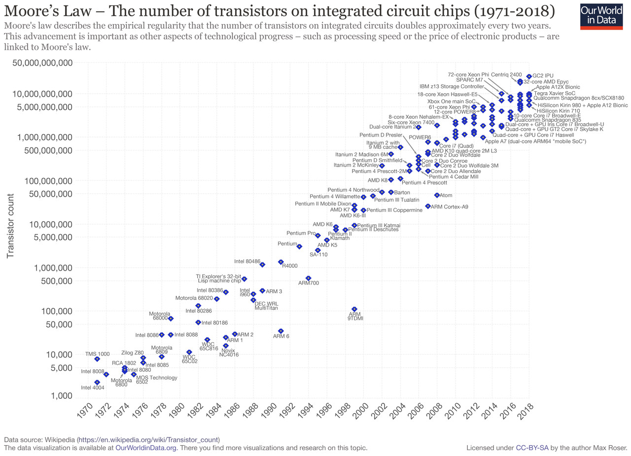
"Moore's Law" is a term coined in 1965 by Gordon Moore, who presented a paper which predicts that semiconductor scaling will allow integrated circuits to feature twice as many transistors present per same area as opposed to a chip manufactured two years ago. That means we could get same performance at half the power than the previous chip, or double the performance at same power/price in only two years time. Today we'll investigate if Moore's Law stayed true to its cause over the years and how much longer can it keep going. For a period longer than five decades the rule of Moore's Law has worked, making the above graph look almost linear if a line would be drawn. What draws the line away from its linearity are occasional hiccups in manufacturing that the industry had to deal with and did overcome in the end. Through history, Moore's Law has been declared and predicted to be dead many times, as the industry approached sub-micron sizes. Starting from 1 µm, many people became skeptical in the law's viability and how well would it hold up, but time has proved these people wrong and we are now already using products that are based on 7 nm node.
The challenge
What really is trying to stop the law are three things: lithography, impurities and economies of scale.
First problem to address are impurities found at the atom level. Silicon manufacturing foundries are melting quartz sand to form a big crystal structure that is cut up into wafers. When sand is melted, impurities are inevitable. That is due to the fact that heating silicon makes it easily react with the halogens (fluorine, chlorine, bromine, and iodine) to form halides. Those halides are removed by using more chemicals that dissolve and remove them so a big crystal can be extracted for making of wafers. "What's the problem caused by removal of these impurities?", you might ask. The smaller the size of an individual transistor, chances are better that even a small atom of impurities, left over from previous cleaning, will be present and render a transistor unusable.
The second problem to address is lithography. In order to make the transistors, you have to "print" them on a silicon wafer. That is done by shining light through a mold called mask, which penetrates the silicon and etches the pattern into a wafer. Naturally, as you decrease the size of your transistor, you have to make your mask smaller. The smaller the mask, the harder it is to make it (you start to notice a certain pattern here with size decreases). So to solve this problem, the semiconductor industry has made a multi-patterning technique which takes several turns into the etching process in order to boost the efficiency of the mask application. However, often times this approach is not enough and UV light is having trouble printing designs to silicon. That's how Extreme UV or EUV lithography was born. It uses a stronger light source with a shorter wavelength to better etch the design and thus reduce the errors the printing might encounter. What the problem really is here, is not the light that passes through the mask, it is the mask itself. The mask is the critical design element as it transfers your design to silicon. If you can not make precise and small masks, you can not get a working chip. Thus, the making of the mask is another critical step that makes Moore's law hard.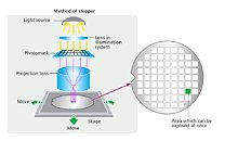 The third and final problem is economics of scale. That is where the less known Moore's second law comes in, which predicts that the cost of setting up a new manufacturing facility is also getting two times more expensive every two years. Today in order to build a new fab, companies are spending billions of dollars. Intel has invested more than $12B in its fab number 42 in Arizona, supposed to manufacture 7 nm chips some day. In addition to the huge capital needed to just open a new fab, companies need to develop its own semiconductor node process. To put things into perspective, industry speculations are that starting from 5 nm and below, over five billion dollars are needed for R&D alone. This is the reason why only three foundries are left manufacturing 7 nm and below - Samsung, Intel, and TSMC.
The way forward
For all the companies that have capital to invest in new manufacturing facilities and equipment, there are quite a few options to choose from in order to keep the law going. Adding new materials, making new kinds of transistors, and stepping into the 3rd dimension.
Knowingly introducing small amounts of other materials into with silicon ("doping") can be a double-edged sword. A new material can boost properties of the transistor, but prove incredibly difficult to manufacture. That is what Intel's experience with cobalt was. They added it to the 10 nm node to decrease resistance in extremely small wires connecting the transistors. Copper is usually used for these wires, but as it is packed into smaller wires, it tends to become more resistive, so cobalt is added beacuse at the same size, Intel found that it is has half the resistance than similar wires made from copper. This addition proved to be useful, but quite difficult to manufacture and it yielded poorly, leading to delays in the new process. Despite the delays, its addition solved a big problem engineers faced, showing the potential of integrating new materials to boost performance. If you remenber, aluminium was used for some time before the industry switched to copper for better performance charactertistics. That transition didn't go smoothly either, but it turned out quite well after a bit of time.
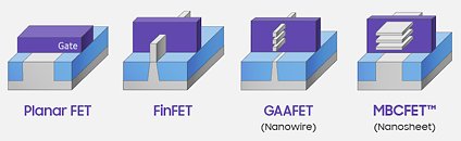
New kinds of transistors are also an option. For a while the industry used standard, planar CMOS FET as a base transistor, which worked fine until we couldn't control current that passes through the transistor, making random switches that often resulted in errors. Just recently, new design called FinFET replaced planar FET, where the fin was raised and the gate started surrounding the source to better control if the transistor will switch or not. In the image below you can see the difference that appeared with introduction of FinFET, allowing manufacturers to make smaller transistors and most importantly control them.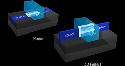 The latest approach to making transistor is "Gate All Around FET" or GAAFET in short. Its design wraps the whole source with a gate, to prevent any possible switches without intent. Planned for use in 5 nm and below, GAAFET is a technology we will see very soon. It will allow even smaller transistor designs with easier manipulation of turning on/off.
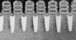
And last but not the least is the 3rd dimension. When we step below 1 nm and start measuring node size in picometers, many forces will prevent transistors from getting smaller. You can go small but you can't break the rules of physics. Quantum tunneling is more present at smaller distances, so at one point we can not go smaller in design without having the transistor make the switch at random times. So when we hit the limits, there is still one place where transistors can be put and that is the vertical axis. If we stack transistors on top of each other, we can automatically double, triple or even quadruple the number of transistors per square millimeter, making the potential of this approach quite big. We already use this technology on HBM memory, and it is about to transfer to logic as well. TSMC also makes Wafer-on-Wafer packages which allow for stacking wafers on top of each other, so it isn't impossible to go 3D and pack more performance in same area, but heat, especially heat density can become a problem.
Summing it all up
My personal opinion is that Moore's Law will not end soon. Not this year, not the one following, nor 2025, when Gordon Moore himself predicts the law to end. It isn't going to be an easy fight for silicon manufacturers, but new technologies are already being worked on and some of them will be deployed very soon, like GAAFET, cobalt, and Wafer-on-Wafer which will allow for additional performance improvements. Chip packaging is getting very good with the appearance of chiplets, making system design seem more like a LEGO building, rather than chip design, were you can pack many different chips next to each other, without the need for a PCB between them.
The thing about Moore's law getting hard to follow is that manufacturers have to get creative if they want to compete and make more money, and that gives this challenge a certain beauty which is only visible if we look at the bigger picture and realize that the best and most interesting solutions are to follow the seemingly boring years of easy performance gain.
Source:
Wikipedia, Samsung (Images)
The challenge
What really is trying to stop the law are three things: lithography, impurities and economies of scale.
First problem to address are impurities found at the atom level. Silicon manufacturing foundries are melting quartz sand to form a big crystal structure that is cut up into wafers. When sand is melted, impurities are inevitable. That is due to the fact that heating silicon makes it easily react with the halogens (fluorine, chlorine, bromine, and iodine) to form halides. Those halides are removed by using more chemicals that dissolve and remove them so a big crystal can be extracted for making of wafers. "What's the problem caused by removal of these impurities?", you might ask. The smaller the size of an individual transistor, chances are better that even a small atom of impurities, left over from previous cleaning, will be present and render a transistor unusable.
The second problem to address is lithography. In order to make the transistors, you have to "print" them on a silicon wafer. That is done by shining light through a mold called mask, which penetrates the silicon and etches the pattern into a wafer. Naturally, as you decrease the size of your transistor, you have to make your mask smaller. The smaller the mask, the harder it is to make it (you start to notice a certain pattern here with size decreases). So to solve this problem, the semiconductor industry has made a multi-patterning technique which takes several turns into the etching process in order to boost the efficiency of the mask application. However, often times this approach is not enough and UV light is having trouble printing designs to silicon. That's how Extreme UV or EUV lithography was born. It uses a stronger light source with a shorter wavelength to better etch the design and thus reduce the errors the printing might encounter. What the problem really is here, is not the light that passes through the mask, it is the mask itself. The mask is the critical design element as it transfers your design to silicon. If you can not make precise and small masks, you can not get a working chip. Thus, the making of the mask is another critical step that makes Moore's law hard.

The way forward
For all the companies that have capital to invest in new manufacturing facilities and equipment, there are quite a few options to choose from in order to keep the law going. Adding new materials, making new kinds of transistors, and stepping into the 3rd dimension.
Knowingly introducing small amounts of other materials into with silicon ("doping") can be a double-edged sword. A new material can boost properties of the transistor, but prove incredibly difficult to manufacture. That is what Intel's experience with cobalt was. They added it to the 10 nm node to decrease resistance in extremely small wires connecting the transistors. Copper is usually used for these wires, but as it is packed into smaller wires, it tends to become more resistive, so cobalt is added beacuse at the same size, Intel found that it is has half the resistance than similar wires made from copper. This addition proved to be useful, but quite difficult to manufacture and it yielded poorly, leading to delays in the new process. Despite the delays, its addition solved a big problem engineers faced, showing the potential of integrating new materials to boost performance. If you remenber, aluminium was used for some time before the industry switched to copper for better performance charactertistics. That transition didn't go smoothly either, but it turned out quite well after a bit of time.
New kinds of transistors are also an option. For a while the industry used standard, planar CMOS FET as a base transistor, which worked fine until we couldn't control current that passes through the transistor, making random switches that often resulted in errors. Just recently, new design called FinFET replaced planar FET, where the fin was raised and the gate started surrounding the source to better control if the transistor will switch or not. In the image below you can see the difference that appeared with introduction of FinFET, allowing manufacturers to make smaller transistors and most importantly control them.


Summing it all up
My personal opinion is that Moore's Law will not end soon. Not this year, not the one following, nor 2025, when Gordon Moore himself predicts the law to end. It isn't going to be an easy fight for silicon manufacturers, but new technologies are already being worked on and some of them will be deployed very soon, like GAAFET, cobalt, and Wafer-on-Wafer which will allow for additional performance improvements. Chip packaging is getting very good with the appearance of chiplets, making system design seem more like a LEGO building, rather than chip design, were you can pack many different chips next to each other, without the need for a PCB between them.
The thing about Moore's law getting hard to follow is that manufacturers have to get creative if they want to compete and make more money, and that gives this challenge a certain beauty which is only visible if we look at the bigger picture and realize that the best and most interesting solutions are to follow the seemingly boring years of easy performance gain.
33 Comments on Moore's Law - Is it Really Dead ?
While great engineers in this industry also claim that this law basically keeps going, internet comments and videos by people who have no idea how silicon engineering works claim otherwise, and sometimes i'm finding myself really confused not knowing who to believe.
Just as a bit of an illustration (data courtesy of Wikichip):
This assumes Intel's 45 nm density in 2006 as an arbitrary starting point, but the results can only get worse if we look back longer than this.
Not even a little. Moore’s Law is not dead, and we will elaborate on our plan to continue it over time. My observation is that the end has always been near, but there has always been and always will be new things we can do to keep pushing that end out. The real challenge is, what happens as we continue to scale technology? What new architecture do we need and how do the problems change? That’s the interesting place.
www.hpcwire.com/2019/03/21/interview-with-2019-person-to-watch-jim-keller/
Die Size251 mm²
41,0 Mtr/mm²
Navi Jul 7th, 2019 Transistors5,700 million
Die Size232 mm²
24,5 Mtr/mm²
3 years = 1.66 performance and density improvement. dead.
The scaling is 80.7% (not 1.66x or 66%)
You can't compare process nodes across different foundries. Polaris was produced by Glofo, Navi is produced by TSMC. The "nm" name given to an individual process node is largely a marketing term meant to indicate progress, not representative of a linear shrink compared to a prior node.
"How about this,
Bulldozer had 1.3x more transistors than phenom at the same "total" performance (8vs6) but were actually %20 slower core to core."
But no, despite both of these examples, exceptions don't break the rules
This PDF shows transistor count and size from 1971 to 2013.
Somebody with time could do the map and fill in 2013 - 2019 with a little research.
www.wagnercg.com/Portals/0/FunStuff/AHistoryofMicroprocessorTransistorCount.pdf
I'll give Mr. G Moore an easy 6-12 month leeway personally. close enough for me. Gotta have some margin of error. Economics alone could hold back any technology from moving forwards.
The current single thread performance is only 2.5x between my i7-920 system and the top of the line systems now.
I bought those in 2009.
my 3930k is only a 1.5x difference.
Those are at stock clocks; my processors are seeing much better performance than the benchmarks I'm quoting.
Video cards have seen a lot of growth; In 2009 I was using a HD4870; there were great increases thru the 5870, 7970, Crossfire, etc.
My last video upgrade was to an RX480, to get rid of all the heat from the 7970x2 crossfire setup. :)
But the death of Gamespy pretty much killed the year to year improvements for me, as all the games moved to "Developed for Xbox" instead of real gaming, like Crysis Wars.
Even the better games now are just Xbox handmedowns.
I had a lot of hope for DOOM, but between the levelup BS and the cheaters, there's no fun playing; we still stick with playing old games on LAN or VPN with closed servers.
Doom arcade mode, on Ultra-violence, is a lot of fun. :)
The most gaming fun I've had in years was the new Sigil levels released for Ultimate Doom; until we get away from the grinding games written by art institute rejects, there's no driver for new hardware for me.
If they want me to upgrade, put out a new, decent FPS with great graphics, a real anticheating system, developed for top end hardware, and M$ will have to release a real OS.
I don't see any of that happening, lol.