News Posts matching #CXL 3.0

Return to Keyword Browsing

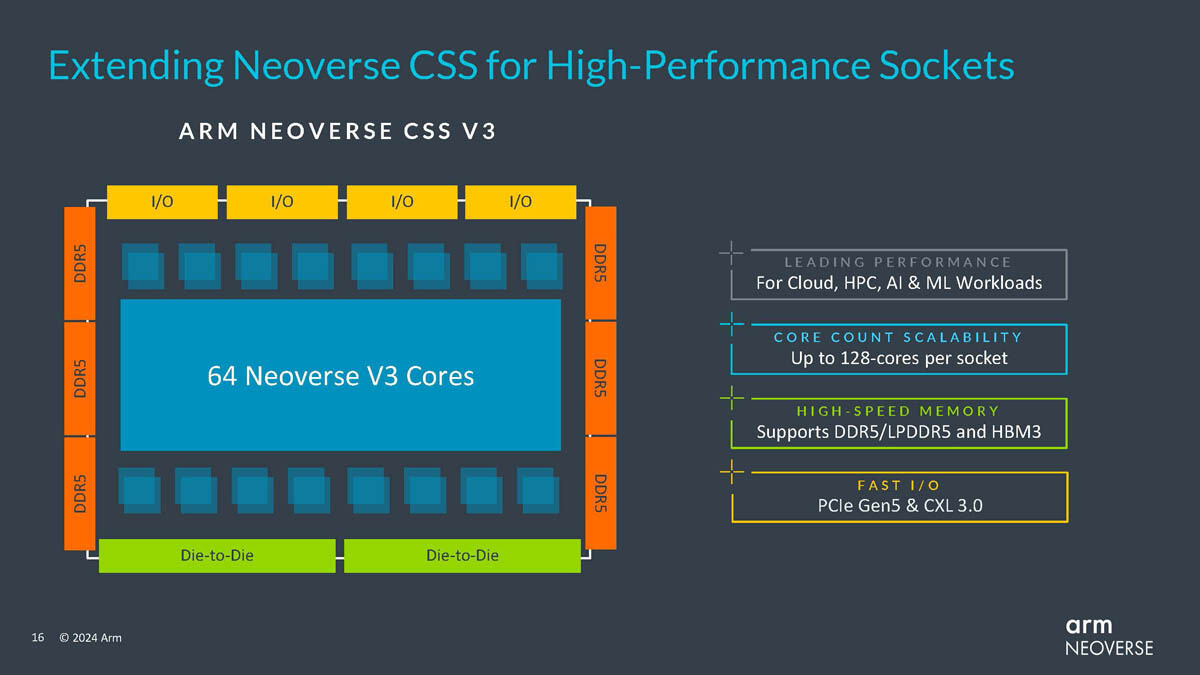
Arm Launches Next-Generation Neoverse CSS V3 and N3 Designs for Cloud, HPC, and AI Acceleration

Last year, Arm introduced its Neoverse Compute Subsystem (CSS) for the N2 and V2 series of data center processors, providing a reference platform for the development of efficient Arm-based chips. Major cloud service providers like AWS with Graviton 4 and Trainuium 2, Microsoft with Cobalt 100 and Maia 100, and even NVIDIA with Grace CPU and Bluefield DPUs are already utilizing custom Arm server CPU and accelerator designs based on the CSS foundation in their data centers. The CSS allows hyperscalers to optimize Arm processor designs specifically for their workloads, focusing on efficiency rather than outright performance. Today, Arm has unveiled the next generation CSS N3 and V3 for even greater efficiency and AI inferencing capabilities. The N3 design provides up to 32 high-efficiency cores per die with improved branch prediction and larger caches to boost AI performance by 196%, while the V3 design scales up to 64 cores and is 50% faster overall than previous generations.

Both the N3 and V3 leverage advanced features like DDR5, PCIe 5.0, CXL 3.0, and chiplet architecture, continuing Arm's push to make chiplets the standard for data center and cloud architectures. The chiplet approach enables customers to connect their own accelerators and other chiplets to the Arm cores via UCIe interfaces, reducing costs and time-to-market. Looking ahead, Arm has a clear roadmap for its Neoverse platform. The upcoming CSS V4 "Adonis" and N4 "Dionysus" designs will build on the improvements in the N3 and V3, advancing Arm's goal of greater efficiency and performance using optimized chiplet architectures. As more major data center operators introduce custom Arm-based designs, the Neoverse CSS aims to provide a flexible, efficient foundation to power the next generation of cloud computing.

Alphawave Semi Partners with Keysight to Deliver a Complete PCIe 6.0 Subsystem Solution

Alphawave Semi (LSE: AWE), a global leader in high-speed connectivity for the world's technology infrastructure, today announced successful collaboration with Keysight Technologies, a market-leading design, emulation, and test solutions provider, demonstrating interoperability between Alphawave Semi's PCIe 6.0 64 GT/s Subsystem (PHY and Controller) Device and Keysight PCIe 6.0 64 GT/s Protocol Exerciser, negotiating a link to the maximum PCIe 6.0 data rate. Alphawave Semi, already on the PCI-SIG 5.0 Integrators list, is accelerating next-generation PCIe 6.0 Compliance Testing through this collaboration.

Alphawave Semi's leading-edge silicon implementation of the new PCIe 6.0 64 GT/s Flow Control Unit (FLIT)-based protocol enables higher data rates for hyperscale and data infrastructure applications. Keysight and Alphawave Semi achieved another milestone by successfully establishing a CXL 2.0 link setting the stage for future cache coherency in the datacenter.

Fujitsu Details Monaka: 150-core Armv9 CPU for AI and Data Center

Ever since the creation of A64FX for the Fugaku supercomputer, Fujitsu has been plotting the development of next-generation CPU design for accelerating AI and general-purpose HPC workloads in the data center. Codenamed Monaka, the CPU is the latest creation for TSMC's 2 nm semiconductor manufacturing node. Based on Armv9-A ISA, the CPU will feature up to 150 cores with Scalable Vector Extensions 2 (SVE2), so it can process a wide variety of vector data sets in parallel. Using a 3D chiplet design, the 150 cores will be split into different dies and placed alongside SRAM and I/O controller. The current width of the SVE2 implementation is unknown.

The CPU is designed to support DDR5 memory and PCIe 6.0 connection for attaching storage and other accelerators. To bring cache coherency among application-specific accelerators, CXL 3.0 is present as well. Interestingly, Monaka is planned to arrive in FY2027, which starts in 2026 on January 1st. The CPU will supposedly use air cooling, meaning the design aims for power efficiency. Additionally, it is essential to note that Monaka is not a processor that will power the post-Fugaku supercomputer. The post-Fugaku supercomputer will use post-Monaka design, likely iterating on the design principles that Monaka uses and refining them for the launch of the post-Fugaku supercomputer scheduled for 2030. Below are the slides from Fujitsu's presentation, in Japenese, which highlight the design goals of the CPU.

Alphawave IP Achieves Its First Testchip Tapeout for TSMC N3E Process

Alphawave IP (LSE: AWE), a global leader in high-speed connectivity for the world's technology infrastructure, today announced the successful tapeout of its ZeusCORE100 1-112 Gbps NRZ/PAM4 Serialiser-Deserialiser ("SerDes"), Alphawave's first testchip on TSMC's most advanced N3E process. Alphawave IP will be exhibiting this new product alongside its complete portfolio of high-performance IP, chiplet, and custom silicon solutions at the TSMC OIP Forum on October 26 in Santa Clara, CA as the Platinum sponsor.

ZeusCORE100 is Alphawave's most advanced multi-standard-SerDes, supporting extra-long channels over 45dB and the most requested standards such as 800G Ethernet, OIF 112G-CEI, PCIe GEN6, and CXL 3.0. Attendees will be able to visit the Alphawave booth and meet the company's technology experts including members of the recently acquired OpenFive team. OpenFive is a longstanding partner of TSMC through the OIP Value Chain Aggregator (VCA) program. OpenFive is one of a select few companies with an idea-to-silicon methodology in TSMC's latest technologies, and advanced packaging capabilities, enabling access to the most advanced foundry solution available with the best Power-Performance-Area (PPA). With Alphawave's industry-leading IP portfolio and the addition of OpenFive's capabilities, designers can create systems on a chip (SoCs) that pack more compute power into smaller form factors for networking, AI, storage, and high-performance computing (HPC) applications.

Rambus Delivers PCIe 6.0 Interface Subsystem for High-Performance Data Center and AI SoCs

Rambus Inc., a premier chip and silicon IP provider making data faster and safer, today announced the availability of its PCI Express (PCIe) 6.0 Interface Subsystem comprised of PHY and controller IP. The Rambus PCIe Express 6.0 PHY also supports the latest version of the Compute Express Link (CXL) specification, version 3.0. "The rapid advancement of AI/ML and data-intensive workloads is driving the continued evolution of data center architectures requiring ever higher levels of performance," said Scott Houghton, general manager of Interface IP at Rambus. "The Rambus PCIe 6.0 Interface Subsystem supports the performance requirements of next-generation data centers with premier latency, power, area and security."

The Rambus PCIe 6.0 Interface Subsystem delivers data rates of up to 64 Gigatransfers per second (GT/s) and has been fully optimized to meet the needs of advanced heterogenous computing architectures. Within the subsystem, the PCIe controller features an Integrity and Data Encryption (IDE) engine dedicated to protecting the PCIe links and the valuable data transferred over them. On the PHY side, full support for CXL 3.0 is available to enable chip-level solutions for cache-coherent memory sharing, expansion and pooling.

CXL Consortium Releases Compute Express Link 3.0 Specification to Expand Fabric Capabilities and Management

The CXL Consortium, an industry standards body dedicated to advancing Compute Express Link (CXL) technology, today announced the release of the CXL 3.0 specification. The CXL 3.0 specification expands on previous technology generations to increase scalability and to optimize system level flows with advanced switching and fabric capabilities, efficient peer-to-peer communications, and fine-grained resource sharing across multiple compute domains.

"Modern datacenters require heterogenous and composable architectures to support compute intensive workloads for applications such as Artificial Intelligence and Machine Learning - and we continue to evolve CXL technology to meet industry requirements," said Siamak Tavallaei, president, CXL Consortium. "Developed by our dedicated technical workgroup members, the CXL 3.0 specification will enable new usage models in composable disaggregated infrastructure."
Return to Keyword Browsing
May 17th, 2024 13:32 EDT change timezone

New Forum Posts

Popular Reviews

Controversial News Posts