News Posts matching #CoPoS

Return to Keyword Browsing

TSMC is Reportedly Considering 3D DRAM Production

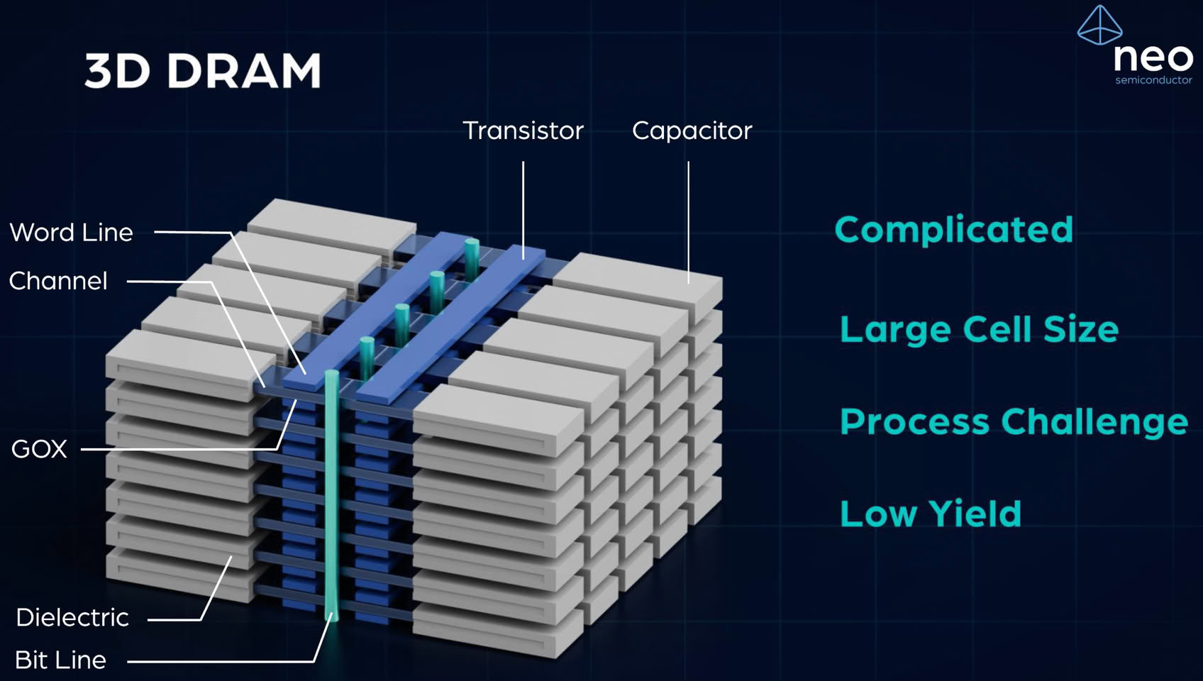
The world's largest chipmaker, TSMC, is reportedly considering entering the memory sector with the manufacturing of advanced DRAM technologies. According to a report from The Information, which cites sources close to the plans, TSMC is contemplating starting the production of 3D DRAM. As we know, there is a desperate need for more DRAM output from the three major memory makers: SK Hynix, Samsung, and Micron. New manufacturing capacity is being developed, but even when it comes online, there might still be a supply imbalance. According to The Information, TSMC is considering 3D DRAM manufacturing at the request of its largest customer, NVIDIA.

Conventional DRAM is currently produced by the big three, with plans to advance into 3D DRAM production beyond what HBM currently offers. To effectively scale memory, the 3D approach is the only way forward, as Micron recently confirmed. Micron has decided not to bring 4F² DRAM to market, even though it claims to have invented the cell design and has been researching it for around two decades, opting instead for the path to 3D DRAM. As one of the most experienced silicon manufacturers globally, TSMC is seemingly evaluating this path as well.


NVIDIA Secures TSMC A16 Node for Next-Generation "Feynman" GPUs

According to supply chain sources and those close to TSMC, NVIDIA is already working on prototyping the replacement for its "Rubin" and "Rubin Ultra" GPU designs with the next-generation "Feynman" GPU microarchitecture. As noted in the latest report from DigiTimes, NVIDIA is opting for TSMC's A16 node, bypassing the N2 family of nodes entirely in favor of the more advanced 1.6 nm A16 design. Mass production is scheduled for the second half of 2028. The "Feynman" designs will rely on the backside power delivery in the A16 node, as well as on packaging technologies like 3D chiplets using SoIC, CoWoS-L 2.5D integration, and next-generation panel-level packaging.

Initially, NVIDIA will use SoIC 3D stacking technology to stack multiple chiplets into a single package, which will shorten the travel time between chips and reduce latency. These 3D chips will then be packaged side-by-side in a CoWoS-L or CoPoS packaging, creating a multi-kilowatt design capable of processing dozens of PetaFLOPS. For memory, NVIDIA will work with its partners to develop customized HBM, likely HBM4E, by the time "Feynman" reaches mass production. This customized memory includes a specialized base die that can contain logic elements like a memory controller or packet processing unit. Think of it as a way to pre-process data before it enters memory, or as a simple speedup, depending on what NVIDIA aims to achieve.

NVIDIA's "Rubin Ultra" Reportedly Faces Issues With CoWoS-L Packaging

NVIDIA is reportedly experiencing manufacturing issues with its next-generation "Rubin Ultra" GPU design, one of the company's most ambitious chip development projects, due to the limitations of modern packaging technology. The world's largest company is already shipping customer samples of the standard "Rubin" GPUs, with mass shipments set to begin this summer. However, the current roadmap for the upgraded "Rubin Ultra" design may be encountering technological limitations, as NVIDIA's design goals are too ambitious for TSMC's packaging capabilities. Reportedly, NVIDIA plans to double the regular "Rubin" two-die package with 8 HBM4 modules into a new "Rubin Ultra" package that will include four silicon dies and 16 HBM4E modules in a single package. This configuration is scheduled for 2027, but the sheer volume of silicon may be too much for TSMC's packaging, according to Global Semi Research.

In a typical CoWoS package, TSMC usually combines multiple smaller dies and multiple HBM memory modules into a unified package that supports the entire AI build-out. However, with the ambitious "Rubin Ultra" design, NVIDIA planned to use CoWoS-L, which was expected to handle the design and concept that "Rubin Ultra" was based on. It is rumored, however, that in a 2+2 die package—meaning four dies as in this architecture—TSMC is encountering warping issues. The package—which includes a substrate—is bending in multiple directions, causing the compute dies of "Rubin Ultra" to not make complete contact with the underlying substrate. This instability means that TSMC has to explore alternatives within its packaging portfolio. One of these alternatives is a panelized approach called CoPoS, which stands for Chip-on-Panel-on-Substrate.

Rapidus Explores Glass Panel-Level Packaging to Rival TSMC

It seems that the Japanese foundry Rapidus is gearing up for strong competition with TSMC. The company has developed a panel-level packaging (PLP) prototype using a glass interposer, with plans to move towards mass production by 2028. At this week's SEMICON Japan 2025 in Tokyo, the prototype will be showcased. It replaces conventional round silicon wafers with large square glass panels, intended for use in high-performance AI packages that combine multi-chip GPUs and more than a dozen of HBM dies. This approach could reduce material waste and enable larger, denser multi-chip assemblies necessary for next-generation AI accelerators, without breaking the traditional laws of 300 mm wafer.

The company is developing 600x600 mm glass panels, which offer a significantly larger usable area than 300 mm silicon wafers and enable the production of more interposers from a single sheet. Glass substrates provide advantages in electrical performance and flatness compared to organic package materials, making them appealing for dense interconnects. However, glass also introduces new manufacturing challenges, such as fragility and potential warpage as panel sizes increase. Intel has notably discontinued its in-house development of glass substrates and has chosen to license the technology to others. The company can thus monetize its innovations, though large-scale Intel-based technology production is not anticipated until after 2030.

TSMC Prepares CoWoS to CoPoS Shift with 750 × 620 mm Panels

TSMC is reportedly preparing to transition its advanced packaging strategy from CoWoS to a panelized approach called CoPoS, which stands for Chip-on-Panel-on-Substrate. The company plans pilot lines as soon as 2026 and aims for mass production between late 2028 and the first half of 2029. The change involves swapping around 300 mm silicon interposers for large square and rectangular panels, with early formats measuring around 310 × 310 mm and later options extending to 515 × 510 mm and even 750 × 620 mm. That larger, square format is intended to reduce wasted edge area, allow bigger reticles and masks for AI accelerators, and make it easier to place more dies and HBM on a single package.

Technically, CoPoS combines CoWoS ideas with fan-out panel-level packaging, building RDL layers on glass or sapphire panels rather than on circular silicon. TSMC is lining up CoPoS development and production at its AP7 Chiayi campus, where phases 4 and 5 are expected to host panel work, and it plans related capacity in future Arizona facilities. Equipment and tooling orders are already being placed, and the supplier list includes global names like KLA and Applied Materials, as well as many Taiwanese manufacturers, such as Innolux. The panel route promises higher area utilization, lower cost per packaged accelerator, and fewer warpage issues as package sizes grow, while TSMC continues to support its existing CoWoS lineup during the transition.

Apple M5 Silicon Adopts LMC Packaging, Paving the Way for CoWoS

According to the well-known Apple insider Ming-Chi Kuo, Apple has reworked a part of its semiconductor supply chain by awarding Taiwan's Eternal Materials exclusive roles in supplying key packaging compounds for its 2026 iPhone and Mac processors. Eternal will supply molding underfill, known as MUF, for the A20 iPhone packages and a liquid molding compound, or LMC, for the high-end M5 Mac processors. TSMC has completed the qualification of these materials and validation for CoWoS use is underway, which could lead to initial shipments in 2026 and a larger role for Eternal in 2027 and 2028. This is noteworthy because it places a Taiwanese materials supplier into a space long dominated by Japanese firms and aligns Apple and TSMC around packaging choices that enable higher memory bandwidth and denser compute layouts.

For the iPhone, transitioning from InFO to wafer-level multi-chip module packaging with MUF reduces material consumption. It simplifies assembly by combining underfill and molding into a single wafer-level process, which is expected to improve yields and lower costs. For Macs, adopting CoWoS-compatible LMC for M5 packages provides better structural integrity, enhanced thermal paths, and more consistent manufacturing outcomes, while leaving full CoWoS adoption for future chip generations. Eternal reportedly beat established Japanese suppliers such as Namics and Nagase to win these orders, which could prompt OSAT partners and other manufacturers to trial the new compounds. It also sets a clear path for Apple to scale more complex multi-die designs in the coming years as it prepares the groundwork for CoWoS and later CoPoS-based processors.

TSMC Plans CoPoS and SoIC Advanced Packaging for Arizona Fab

TSMC plans to expand its Arizona facility with advanced packaging by constructing two dedicated buildings near to its Fab 21 complex. The first, Advanced Packaging Facility 1 (AP1), is slated to break ground in 2028 alongside Phase 3 of Fab 21, which will eventually produce chips on the N2 (2 nm) node and potentially the A16 process. A second structure, AP2, will follow in tandem with later expansions (Phases 4 and 5), though exact dates remain unconfirmed. Both sites will focus on System-on-Integrated-Chips (SoIC) and the emerging Chip-on-Panel-on-Substrate (CoPoS) technology. SoIC uses through-silicon vias to stack cache or memory dies directly beneath compute cores, a technique already proven in AMD's Ryzen X3D processors. CoPoS, by contrast, replaces traditional circular wafers with rectangular panels measuring approximately 310x310 mm.

This shift multiplies the usable substrate area by more than five times, enabling the denser integration of high-bandwidth memory stacks, I/O chiplets, and multiple compute tiles while driving down per-unit costs. Behind the scenes, TSMC will kick off a CoPoS pilot line as early as 2026, aiming to complete partner validation by late 2027. This pilot run is designed to address manufacturing challenges and secure design wins with major customers, including NVIDIA, AMD, and Apple, ensuring that US-assembled packages meet the same performance and reliability standards as those in Taiwan. Mass production at AP1 is not expected to ramp up until late 2029 or early 2030, aligning with TSMC's two-year lead-time practice: new node and packaging innovations debut on the home island before being transplanted abroad.

TSMC Prepares "CoPoS": Next-Gen 310 × 310 mm Packages

As demand for ever-growing AI compute power continues to rise and manufacturing advanced nodes becomes more difficult, packaging is undergoing its golden era of development. Today's advanced accelerators often rely on TSMC's CoWoS modules, which are built on wafer cuts measuring no more than 120 × 150 mm in size. In response to the need for more space, TSMC has unveiled plans for CoPoS, or "Chips on Panel on Substrate," which could expand substrate dimensions to 310 × 310 mm and beyond. By shifting from round wafers to rectangular panels, CoPoS offers more than five times the usable area. This extra surface makes it possible to integrate additional high-bandwidth memory stacks, multiple I/O chiplets and compute dies in a single package. It also brings panel-level packaging (PLP) to the fore. Unlike wafer-level packaging (WLP), PLP assembles components on large, rectangular panels, delivering higher throughput and lower cost per unit. Systems with PLP will be actually viable for production runs and allow faster iterations over WLP.

TSMC will establish a CoPoS pilot line in 2026 at its Visionchip subsidiary. In 2027, the pilot facility will focus on refining the process, to meet partner requirements by the end of the year. Mass production is projected to begin between the end of 2028 and early 2029 at TSMC's Chiayi AP7 campus. That site, chosen for its modern infrastructure and ample space, is also slated to host production of multi-chip modules and System-on-Wafer technologies. NVIDIA is expected to be the launch partner for CoPoS. The company plans to leverage the larger panel area to accommodate up to 12 HBM4 chips alongside several GPU chiplets, offering significant performance gains for AI workloads. At the same time, AMD and Broadcom will continue using TSMC's CoWoS-L and CoWoS-R variants for their high-end products. Beyond simply increasing size, CoPoS and PLP may work in tandem with other emerging advances, such as glass substrates and silicon photonics. If development proceeds as planned, the first CoPoS-enabled devices could reach the market by late 2029.
Return to Keyword Browsing
Nov 12th, 2026 07:36 PST change timezone

New Forum Posts

Popular Reviews

TPU on YouTube

Controversial News Posts