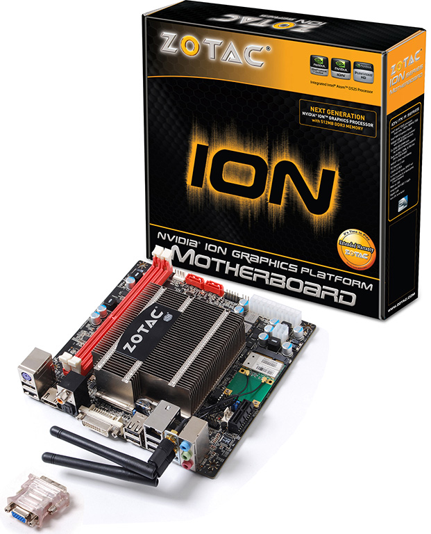
ONFI Announces Publication of 3.0 Standard, Pushes Data Transfer Speeds to 400 MB/sec
The Open NAND Flash Interface (ONFI) Working Group, the organization dedicated to simplifying integration of NAND Flash memory into consumer electronic devices, computing platforms, and industrial systems, today published the new ONFI 3.0 standard. By using the non-volatile DDR2 (NV-DDR2) interface, the newly ratified standard reaches speeds of up to 400 megabytes (MB)/sec, doubling the current NAND interface transfer rates.
The ONFI 3.0 standard details the interface and infrastructure that ONFI's more than 100 members can employ to develop products that deliver the industry's fastest NAND interface. Improvements in ONFI 3.0's NAND interface speeds will also enable future NAND controllers to achieve similar performance with half the number of channels, providing both a cost and space savings, which are key requirements for solid-state drive (SSD) design. The ONFI 3.0 incorporates a sophisticated die selection feature that reduces the number of chip enable (CE) pins, which in turn lowers the number of controller pins making PCB routing more efficient. Reducing the number of CE pins is especially important for SSDs, providing a significant cost reduction and allowing the extra pins to be assigned to other applications within the system.
The ONFI 3.0 standard details the interface and infrastructure that ONFI's more than 100 members can employ to develop products that deliver the industry's fastest NAND interface. Improvements in ONFI 3.0's NAND interface speeds will also enable future NAND controllers to achieve similar performance with half the number of channels, providing both a cost and space savings, which are key requirements for solid-state drive (SSD) design. The ONFI 3.0 incorporates a sophisticated die selection feature that reduces the number of chip enable (CE) pins, which in turn lowers the number of controller pins making PCB routing more efficient. Reducing the number of CE pins is especially important for SSDs, providing a significant cost reduction and allowing the extra pins to be assigned to other applications within the system.