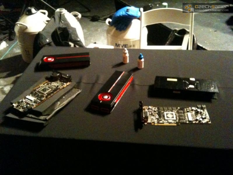
AMD Cypress ''Radeon HD 5870'' Stripped
Here are the first pictures of the obverse side of Cypress' PCB, and the first pictures of the centre of attraction: the AMD Cypress GPU. CzechGamer dissembled two Cypress "Radeon HD 5870" cards for a quick blurrycam photo-session. The PCB shot reveals quite a bit about Cypress, particularly about the GPU.
To begin with, the GPU is AMD's overhaul on transistor counts, and a bold work of engineering on the 40 nm manufacturing process, given the kind of problems foundry partners had initially. Apparently they seem to have recovered with most of them, as AMD's AIB partners are coming up with new products based on the 40 nm RV740 GPU on a weekly basis. The package holds a "diamond-shaped" die that is angled in a way similar to RV740, RV730, or more historically, the R600. The seemingly huge die measures 338 mm² (area), and for 40 nm, it translates to "huge", and is vindicated by the transistor count of ~2.1 billion. In contrast, AMD's older flagship GPU, the RV790 holds 959 million, and NVIDIA's GT200 holds 1.4 billion.
To begin with, the GPU is AMD's overhaul on transistor counts, and a bold work of engineering on the 40 nm manufacturing process, given the kind of problems foundry partners had initially. Apparently they seem to have recovered with most of them, as AMD's AIB partners are coming up with new products based on the 40 nm RV740 GPU on a weekly basis. The package holds a "diamond-shaped" die that is angled in a way similar to RV740, RV730, or more historically, the R600. The seemingly huge die measures 338 mm² (area), and for 40 nm, it translates to "huge", and is vindicated by the transistor count of ~2.1 billion. In contrast, AMD's older flagship GPU, the RV790 holds 959 million, and NVIDIA's GT200 holds 1.4 billion.