News Posts matching #Fraunhofer IPMS

Return to Keyword Browsing

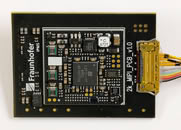
Fraunhofer IPMS Develops Compact 2K OLED Microdisplay Package with MIPI DSI-2

Researchers at the Fraunhofer Institute for Photonic Microsystems IPMS have developed a new compact package for their 2K OLED microdisplay. The microdisplay package integrates MIPI DSI-2 control and the generation of all required display voltages. The new solution will be presented for the first time at SEMICON Europa 2026 from November 10 to 13, 2026, in Munich - at the Silicon Saxony joint booth in Hall B1, Booth B1-221-25.

OLED microdisplays are frequently used in portable applications such as helmets and smart glasses as well as in optical devices. The new microdisplay package simplifies the integration of Fraunhofer IPMS's 2K microdisplays into such systems, as it combines the microdisplay with the complete electronics required for its control. An integrated 20 mm x 20 mm system-on-module (SoM) implements the MIPI DSI-2 interface via D-PHY, which is widely used in mobile processors and transmits image data and control commands serially at high speeds. The microdisplay package supports up to four data lanes with a data rate of up to 2.5 Gbit/s per lane.

Fraunhofer IPMS Develops High-Density Chiplet Systems at the Wafer Level

Breakthrough in chip manufacturing: As part of the European APECS pilot line, researchers at Fraunhofer Institute for Photonic Microsystems IPMS have developed a method that allows different chip components to be fused almost seamlessly into a single unit. By precisely embedding small chiplets into specially structured silicon pockets, Fraunhofer IPMS succeeded in combining the advantages of a compact single chip with the flexibility of modular systems for the first time. This achievement demonstrates the feasibility of quasi-monolithic integration (QMI) and bridges the gap between traditional chip packaging and cutting-edge semiconductor manufacturing.

Growing demands for greater complexity, computing power and system compactness are calling for a radical rethink of semiconductor manufacturing. The vision for future-proof microelectronics is to create systems that are as powerful as a single chip yet offer the flexibility of modular building blocks. Within the APECS pilot line, which focuses on "Advanced Packaging and Heterogeneous Integration for Electronic Components and Systems", Fraunhofer IPMS is pursuing the quasi-monolithic integration (QMI) approach. The aim is to integrate various chip components, such as control electronics, sensors and microelectromechanical systems (MEMS), at the wafer level, while retaining the benefits of a compact single chip.

Fraunhofer, TSRI Partner on Ferroelectric Transistors for Low-Power Memory ICs

Artificial intelligence works fast, but its energy consumption is growing rapidly. A German-Taiwanese research team is now developing a solution: new memory for leading chip technologies smaller than 3 nm. These innovative nanosheet devices enable computing operations directly in memory, thereby drastically reducing energy consumption. They are based on ferroelectric field-effect transistors (FeMFETs) made from hafnium oxide, which are particularly efficient. With a joint research program, Fraunhofer IPMS, Fraunhofer IMWS, and the Taiwanese research institute TSRI are laying the foundation for the next generation of energy-efficient AI chips - from smartphones and automobiles to medical devices.

Given the rapidly growing demand for artificial intelligence (AI) and neuromorphic computing, the energy consumption of data centers and edge systems is increasing dramatically. A key bottleneck is the transfer of data between main memory and the computing unit. A joint German-Taiwanese project aims to address precisely this issue: innovative memory technology will enable computing "directly in memory", with significantly lower latency and energy consumption.
Return to Keyword Browsing
Nov 17th, 2026 13:47 CST change timezone

New Forum Posts

Popular Reviews

TPU on YouTube

Controversial News Posts