News Posts matching #GH100

Return to Keyword Browsing

Nvidia CEO Reiterates Solid Partnership with TSMC

One key takeaway from the ongoing GTC is that Nvidia's AI empire has taken shape with strong partnerships from TSMC and other Taiwanese makers, such as those major server ODMs.

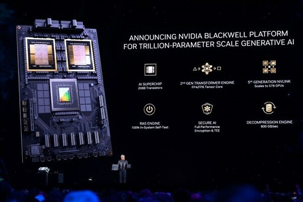
According to the news report from the technology-focused media DIGITIMES Asia, during his keynote at GTC on March 18, Huang underscored his company's partnerships with TSMC, as well as the supply chain in Taiwan. Speaking to the press later, Huang said Nvidia will have a very strong demand for CoWoS, the advanced packaging services TSMC offers.

TSMC Plans to Put a Trillion Transistors on a Single Package by 2030

During the recent IEDM conference, TSMC previewed its process roadmap for delivering next-generation chip packages packing over one trillion transistors by 2030. This aligns with similar long-term visions from Intel. Such enormous transistor counts will come through advanced 3D packaging of multiple chipsets. But TSMC also aims to push monolithic chip complexity higher, ultimately enabling 200 billion transistor designs on a single die. This requires steady enhancement of TSMC's planned N2, N2P, N1.4, and N1 nodes, which are slated to arrive between now and the end of the decade. While multi-chipset architectures are currently gaining favor, TSMC asserts both packaging density and raw transistor density must scale up in tandem. Some perspective on the magnitude of TSMC's goals include NVIDIA's 80 billion transistor GH100 GPU—among today's largest chips, excluding wafer-scale designs from Cerebras.

Yet TSMC's roadmap calls for more than doubling that, first with over 100 billion transistor monolithic designs, then eventually 200 billion. Of course, yields become more challenging as die sizes grow, which is where advanced packaging of smaller chiplets becomes crucial. Multi-chip module offerings like AMD's MI300X and Intel's Ponte Vecchio already integrate dozens of tiles, with PVC having 47 tiles. TSMC envisions this expansion to chip packages housing more than a trillion transistors via its CoWoS, InFO, 3D stacking, and many other technologies. While the scaling cadence has recently slowed, TSMC remains confident in achieving both packaging and process breakthroughs to meet future density demands. The foundry's continuous investment ensures progress in unlocking next-generation semiconductor capabilities. But physics ultimately dictates timelines, no matter how aggressive the roadmap.

Samsung Notes: HBM4 Memory is Coming in 2025 with New Assembly and Bonding Technology

According to the editorial blog post published on the Samsung blog by SangJoon Hwang, Executive Vice President and Head of the DRAM Product & Technology Team at Samsung Electronics, we have information that High-Bandwidth Memory 4 (HBM4) is coming in 2025. In the recent timeline of HBM development, we saw the first appearance of HBM memory in 2015 with the AMD Radeon R9 Fury X. The second-generation HBM2 appeared with NVIDIA Tesla P100 in 2016, and the third-generation HBM3 saw the light of the day with NVIDIA Hopper GH100 GPU in 2022. Currently, Samsung has developed 9.8 Gbps HBM3E memory, which will start sampling to customers soon.

However, Samsung is more ambitious with development timelines this time, and the company expects to announce HBM4 in 2025, possibly with commercial products in the same calendar year. Interestingly, the HBM4 memory will have some technology optimized for high thermal properties, such as non-conductive film (NCF) assembly and hybrid copper bonding (HCB). The NCF is a polymer layer that enhances the stability of micro bumps and TSVs in the chip, so memory solder bump dies are protected from shock. Hybrid copper bonding is an advanced semiconductor packaging method that creates direct copper-to-copper connections between semiconductor components, enabling high-density, 3D-like packaging. It offers high I/O density, enhanced bandwidth, and improved power efficiency. It uses a copper layer as a conductor and oxide insulator instead of regular micro bumps to increase the connection density needed for HBM-like structures.

Comino Launches Water Block for NVIDIA H100 PCIe Accelerator Card

A relatively new player in the water cooling industry, Comino, has recently introduced its latest product: a water block for the NVIDIA H100 PCIe accelerator card. The new block provides full coverage with cooling to the GPU, GDDR, and VRM. In the design, Comino only used non-corrosive materials such as copper, stainless steel, aluminium, and Plastic. The core of the block uses copper, while the frame and backplate use aluminium. The company claims that at a coolant temperature of 20°C, the temperature of the GH100 chip with Comino water blocks will be 30º-40°C.

Comino uses "deformational cutting" technology to create a copper fin as thin as 0.1 mm with a 0.1 mm channel and 3 mm height. In Comino water blocks, micro fins are optimized for a low-pressure drop with a thickness of 0.25 mm, channel - 0.25 mm, and 2.7 mm height. The block itself is a single-slot solution with fitting adapters on the back and a 90º adapter option for workstation implementation. More information is available on the Comino website. You can see the images below.

NVIDIA H100 Hopper GPU Tested for Gaming, Slower Than Integrated GPU

NVIDIA's H100 Hopper GPU is a device designed for pure AI and other compute workloads, with the least amount of consideration for gaming workloads that involve graphics processing. However, it is still interesting to see how this 30,000 USD GPU fairs in comparison to other gaming GPUs and whether it is even possible to run games on it. It turns out that it is technically feasible but not making much sense, as the Chinese YouTube channel Geekerwan notes. Based on the GH100 GPU SKU with 14,592 CUDA, the H100 PCIe version tested here can achieve 204.9 TeraFLOPS at FP16, 51.22 TeraFLOPS at FP32, and 25.61 TeraFLOPS at FP64, with its natural power laying in accelerating AI workloads.

However, how does it fare in gaming benchmarks? Not very well, as the testing shows. It scored 2681 points in 3DMark Time Spy, which is lower than AMD's integrated Radeon 680M, which managed to score 2710 points. Interestingly, the GH100 has only 24 ROPs (render output units), while the gaming-oriented GA102 (highest-end gaming GPU SKU) has 112 ROPs. This is self-explanatory and provides a clear picture as to why the H100 GPU is used for computing only. Since it doesn't have any display outputs, the system needed another regular GPU to provide the picture, while the computation happened on the H100 GPU.

NVIDIA Could Launch Hopper H100 PCIe GPU with 120 GB Memory

NVIDIA's high-performance computing hardware stack is now equipped with the top-of-the-line Hopper H100 GPU. It features 16896 or 14592 CUDA cores, developing if it comes in SXM5 of PCIe variant, with the former being more powerful. Both variants come with a 5120-bit interface, with the SXM5 version using HBM3 memory running at 3.0 Gbps speed and the PCIe version using HBM2E memory running at 2.0 Gbps. Both versions use the same capacity capped at 80 GBs. However, that could soon change with the latest rumor suggesting that NVIDIA could be preparing a PCIe version of Hopper H100 GPU with 120 GBs of an unknown type of memory installed.

According to the Chinese website "s-ss.cc" the 120 GB variant of the H100 PCIe card will feature an entire GH100 chip with everything unlocked. As the site suggests, this version will improve memory capacity and performance over the regular H100 PCIe SKU. With HPC workloads increasing in size and complexity, more significant memory allocation is needed for better performance. With the recent advances in Large Language Models (LLMs), AI workloads use trillions of parameters for tranining, most of which is done on GPUs like NVIDIA H100.

NVIDIA Hopper Whitepaper Reveals Key Specs of Monstrous Compute Processor

The NVIDIA GH100 silicon powering the next-generation NVIDIA H100 compute processor is a monstrosity on paper, with an NVIDIA whitepaper published over the weekend revealing its key specifications. NVIDIA is tapping into the most advanced silicon fabrication node currently available from TSMC to build the compute die, which is TSMC N4 (4 nm-class EUV). The H100 features a monolithic silicon surrounded by up to six on-package HBM3 stacks.

The GH100 compute die is built on the 4 nm EUV process, and has a monstrous transistor-count of 80 billion, a nearly 50% increase over the GA100. Interestingly though, at 814 mm², the die-area of the GH100 is less than that of the GA100, with its 826 mm² die built on the 7 nm DUV (TSMC N7) node, all thanks to the transistor-density gains of the 4 nm node over the 7 nm one.

NVIDIA H100 is a Compute Monster with 80 Billion Transistors, New Compute Units and HBM3 Memory

During the GTC 2022 keynote, NVIDIA announced its newest addition to the accelerator cards family. Called NVIDIA H100 accelerator, it is the company's most powerful creation ever. Utilizing 80 billion of TSMC's 4N 4 nm transistors, H100 can output some insane performance, according to NVIDIA. Featuring a new fourth-generation Tensor Core design, it can deliver a six-fold performance increase compared to A100 Tensor Cores and a two-fold MMA (Matrix Multiply Accumulate) improvement. Additionally, new DPX instructions accelerate Dynamic Programming algorithms up to seven times over the previous A100 accelerator. Thanks to the new Hopper architecture, the Streaming Module structure has been optimized for better transfer of large data blocks.

The full GH100 chip implementation features 144 SMs, and 128 FP32 CUDA cores per SM, resulting in 18,432 CUDA cores at maximum configuration. The NVIDIA H100 GPU with SXM5 board form-factor features 132 SMs, totaling 16,896 CUDA cores, while the PCIe 5.0 add-in card has 114 SMs, totaling 14,592 CUDA cores. As much as 80 GB of HBM3 memory surrounds the GPU at 3 TB/s bandwidth. Interestingly, the SXM5 variant features a very large TDP of 700 Watts, while the PCIe card is limited to 350 Watts. This is the result of better cooling solutions offered for the SXM form-factor. As far as performance figures are concerned, the SXM and PCIe versions provide two distinctive figures for each implementation. You can check out the performance estimates in various precision modes below. You can read more about the Hopper architecture and what makes it special in this whitepaper published by NVIDIA.
NVIDIA H100

NVIDIA Announces Hopper Architecture, the Next Generation of Accelerated Computing

GTC—To power the next wave of AI data centers, NVIDIA today announced its next-generation accelerated computing platform with NVIDIA Hopper architecture, delivering an order of magnitude performance leap over its predecessor. Named for Grace Hopper, a pioneering U.S. computer scientist, the new architecture succeeds the NVIDIA Ampere architecture, launched two years ago.

The company also announced its first Hopper-based GPU, the NVIDIA H100, packed with 80 billion transistors. The world's largest and most powerful accelerator, the H100 has groundbreaking features such as a revolutionary Transformer Engine and a highly scalable NVIDIA NVLink interconnect for advancing gigantic AI language models, deep recommender systems, genomics and complex digital twins.

First Pictures of NVIDIA "Hopper" H100 Compute Processor Surface

Here's the first picture of an NVIDIA H100 "Hopper" compute processor, which succeeds the two-year old "Ampere" A100. The "Hopper" compute architecture doubles down on the strengths of "Ampere," in having the most advanced AI deep-learning compute machinery, FP64 math capability, and lots more. Built on the TSMC N5 (5 nm) node, the "GH100" processor more than doubles the transistor-count over the A100, which is expected to be around 140 billion.

Unlike the A100, the H100 will come with graphics rendering capability, The GH100 is one of the first NVIDIA chips to feature two different kinds of GPCs. Of the six GPCs has NVIDIA's graphics-relevant SMs, whereas the other GPCs have compute-relevant SMs. The graphics SM will have components such as RT cores, and other raster machinery; while the compute SMs will have specialized tensor cores and FP64 SIMD units. Counting the graphics SM, there are a total of 144 SMs on the silicon. Memory is care of what could be a 6144-bit HBM3 interface. NVIDIA will build various products based on the "GH100," including SXM cards, DGX Stations, SuperPods, and even PCIe add-in cards (AICs). NVIDIA is expected to unveil the H100 later today.

NVIDIA to Split Graphics and Compute Architecture Naming, "Blackwell" Architecture Spotted

The recent NVIDIA data-leak springs up information on various upcoming graphics parts. Besides "Ada Lovelace," "Hopper," we come across a new codename, "Blackwell." It turns out that NVIDIA is splitting the the graphics and compute architecture naming with the next generation, not unlike what AMD did, with its RDNA and CDNA series. The current "Ampere" architecture is being used both for compute and graphics, with the streaming multiprocessor for the two being slightly different—the compute "Ampere" has more FP64 and Tensor components, while the graphics "Ampere" does away with these in favor of RT cores and graphics-relevant components.

The graphics architecture to succeed GeForce "Ampere" will be GeForce "Ada Lovelace." GPUs in this series are identified in the leaked code as "AD102," "AD103," "AD104," "AD106," "AD107," and "AD10B," succeeding a similar numbering for parts with the "A" (GeForce Ampere) series. The compute architecture succeeding "Ampere" will be codenamed "Hopper." with parts in the series being codenamed "GH100" and "GH202." Another compute or datacenter architecture is "Blackwell," with parts being codenamed "GB100" and "GB102." From all accounts, NVIDIA is planning to launch the GeForce 40-series "Ada" graphics card lineup in the second half of 2022. The company is in need of a similar refresh for its compute product lineup, and could debut "Hopper" either toward the end of 2022 or next year. "Blackwell" could follow "Hopper."

NVIDIA "Hopper" Might Have Huge 1000 mm² Die, Monolithic Design

Renowned hardware leaker kopike7kimi on Twitter revealed some purported details on NVIDIA's next-generation architecture for HPC (High Performance Computing), Hopper. According to the leaker, Hopper is still sporting a classic monolithic die design despite previous rumors, and it appears that NVIDIA's performance targets have led to the creation of a monstrous, ~1000 mm² die package for the GH100 chip, which usually maxes out the complexity and performance that can be achieved on a particular manufacturing process. This is despite the fact that Hopper is also rumored to be manufactured under TSMC's 5 nm technology, thus achieving higher transistor density and power efficiency compared to the 8 nm Samsung process that NVIDIA is currently contracting. At the very least, it means that the final die will be bigger than the already enormous 826 mm² of NVIDIA's GA100.

If this is indeed the case and NVIDIA isn't deploying a MCM (Multi-Chip Module) design on Hopper, which is designed for a market with increased profit margins, it likely means that less profitable consumer-oriented products from NVIDIA won't be featuring the technology either. MCM designs also make more sense in NVIDIA's HPC products, as they would enable higher theoretical performance when scaling - exactly what that market demands. Of course, NVIDIA could be looking to develop an MCM version of the GH100 still; but if that were to happen, the company could be looking to pair two of these chips together as another HPC product (rumored GH-102). ~2,000 mm² in a single GPU package, paired with increased density and architectural improvements might actually be what NVIDIA requires to achieve the 3x performance jump from the Ampere-based A100 the company is reportedly targeting.
Return to Keyword Browsing
Apr 24th, 2024 20:44 EDT change timezone

New Forum Posts

Popular Reviews

Controversial News Posts