Wednesday, May 4th 2022

NVIDIA Hopper Whitepaper Reveals Key Specs of Monstrous Compute Processor
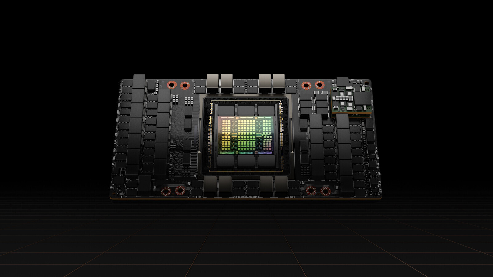
The NVIDIA GH100 silicon powering the next-generation NVIDIA H100 compute processor is a monstrosity on paper, with an NVIDIA whitepaper published over the weekend revealing its key specifications. NVIDIA is tapping into the most advanced silicon fabrication node currently available from TSMC to build the compute die, which is TSMC N4 (4 nm-class EUV). The H100 features a monolithic silicon surrounded by up to six on-package HBM3 stacks.
The GH100 compute die is built on the 4 nm EUV process, and has a monstrous transistor-count of 80 billion, a nearly 50% increase over the GA100. Interestingly though, at 814 mm², the die-area of the GH100 is less than that of the GA100, with its 826 mm² die built on the 7 nm DUV (TSMC N7) node, all thanks to the transistor-density gains of the 4 nm node over the 7 nm one.
 The component hierarchy of the GH100 is similar to that of previous generation NVIDIA architectures. The main number-crunching machinery is spread across 144 streaming multiprocessors (SM). The chip features 18,432 FP32 CUDA cores, and 9,216 double-precision (FP64) CUDA cores. There are also 576 fourth-generation Tensor cores. One of the GPCs on the silicon has raster graphics hardware, so the silicon has certain GPU capabilities.
The GH100 features a 6144-bit HBM3 memory interface, and 80 GB is the standard memory amount for the H100 compute processor. The memory bandwidth on offer is expected to exceed 3 TB/s, including ECC support. The host-interfaces get a major upgrade, too. The SXM form-factor board comes with the latest-generation NVLink interconnect that has 900 GB/s bandwidth.
The AIC (add-in card) form-factor model has PCI-Express 5.0 x16 (128 GB/s). Both interfaces introduce resource-pooling features. Lastly, NVIDIA is pushing up the power envelope in pursuit of performance, with the H100 having a typical power value of 700 W, compared to 400 W of the A100. Interestingly, the H100 does not max out the GH100 silicon, with the high-density SXM form-factor board featuring 132 out of 144 SM, while the PCIe AIC board only has 114 out of 144. Both models could come with clock speeds as high as 1.80 GHz.
Source:
ComputerBase.de
The GH100 compute die is built on the 4 nm EUV process, and has a monstrous transistor-count of 80 billion, a nearly 50% increase over the GA100. Interestingly though, at 814 mm², the die-area of the GH100 is less than that of the GA100, with its 826 mm² die built on the 7 nm DUV (TSMC N7) node, all thanks to the transistor-density gains of the 4 nm node over the 7 nm one.

The GH100 features a 6144-bit HBM3 memory interface, and 80 GB is the standard memory amount for the H100 compute processor. The memory bandwidth on offer is expected to exceed 3 TB/s, including ECC support. The host-interfaces get a major upgrade, too. The SXM form-factor board comes with the latest-generation NVLink interconnect that has 900 GB/s bandwidth.
The AIC (add-in card) form-factor model has PCI-Express 5.0 x16 (128 GB/s). Both interfaces introduce resource-pooling features. Lastly, NVIDIA is pushing up the power envelope in pursuit of performance, with the H100 having a typical power value of 700 W, compared to 400 W of the A100. Interestingly, the H100 does not max out the GH100 silicon, with the high-density SXM form-factor board featuring 132 out of 144 SM, while the PCIe AIC board only has 114 out of 144. Both models could come with clock speeds as high as 1.80 GHz.
8 Comments on NVIDIA Hopper Whitepaper Reveals Key Specs of Monstrous Compute Processor