News Posts matching #GM204

Return to Keyword Browsing

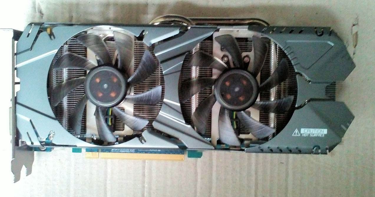
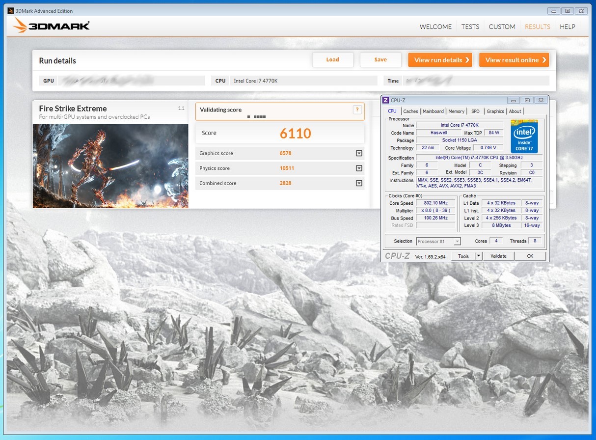
NVIDIA GeForce GTX 980 Reference Board Pictured

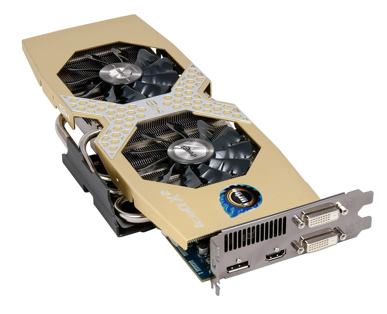
Here are the first pictures of the reference-design GeForce GTX 980 graphics card. This gorgeous looking board is something to get used to, as it could be a while before we see non-reference boards for the GTX 980. Its smaller sibling, the GTX 970, could launch with non-reference design boards right off the bat. Outwardly, the GTX 980 looks exactly like a GeForce GTX 780 reference board, with NVIDIA's space-age cooling shroud.

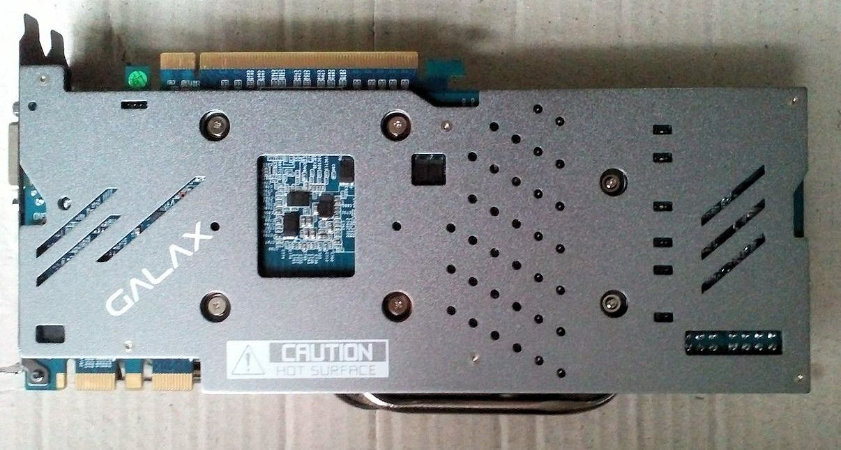
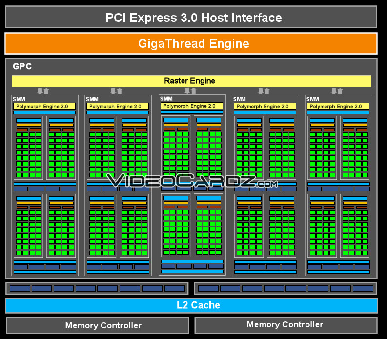
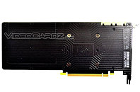
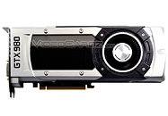
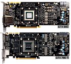
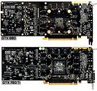
The only difference here is a metal backplate decking up the card. This backplate isn't cooling anything, and traces reveal that the card is indeed holding just 8 memory chips, confirming its 256-bit wide GDDR5 memory interface. The GeForce GTX 980 is based on NVIDIA's new GM204 silicon, a derivative of the company's new "Maxwell" architecture, which made its debut with the GeForce GTX 750 Ti. The package of GM204 looks roughly as big as a GK104. The card draws power from a pair of 6-pin PCIe power connectors, and uses a 4+1 phase VRM to condition power.

Radeon R9 290X Sees Price Cuts

AMD is apparently working with its add-in board manufacturers and retailers to bring down prices of its flagship single-GPU graphics card, the Radeon R9 290X. The card can now be had for as low as $449, non-reference design, factory-overclocked cards starting at a $50 premium. Prices could settle down somewhere between $450 and $500. This closely follows AMD's move to bring down price of its dual-GPU flagship Radeon R9 295X2 by a whopping 34 percent, down to $999, offering performance competitive to the $2999 GeForce GTX TITAN-Z. NVIDIA is preparing two new graphics cards competitive in performance to the Radeon R9 290 series, the GeForce GTX 970 and GTX 980. The two are based on the company's new 28 nm "GM204" silicon, implementing the "Maxwell" GPU architecture.

ZOTAC GeForce GTX 970 Pictured

Here's the first picture of a ZOTAC-branded GeForce GTX 970 graphics card, the first one shot with its box, confirming the GTX 900 series nomenclature NVIDIA adopted. ZOTAC's card appears to be based on a non-reference PCB, and features a rather compact-looking aluminium fin-stack heatsink, which is ventilated by a pair of 80 mm spinners. The box doesn't flash any "OC" markings, so it's safe to assume that he card runs at its reference clock speeds of 1051 MHz core, 1178 MHz GPU Boost, and 7012 MHz (GDDR5-effective) memory. The card features 4 GB of memory across a 256-bit wide memory interface. Based on the 28 nm "GM204" silicon, the GeForce GTX 970 reportedly features 1,664 CUDA cores, 138 TMUs, and 32 ROPs.

MSI Teases GeForce GTX 970 Gaming with TwinFrozr V

MSI showed off the first moneyshot render of its GeForce GTX 970 Gaming graphics card. Trailing an earlier leaked render viewed from the top of the card. The new one reveals MSI giving the TwinFrozr V cooler a bold 2-tone cooler shroud, holding a pair of 100 mm fans that ventilate a chunky copper heat-pipe fed aluminium fin stack. MSI could give the GTX 970 a factory-overclock to take advantage of its meaty cooling solution. Based on the 28 nm GM204 silicon, the GeForce GTX 970 is said to feature 1,664 CUDA cores based on the "Maxwell" architecture, 138 TMUs, 32 ROPs, a 256-bit wide memory interface, and 4 GB of memory. It will launch a little later this month.

Galaxy GeForce GTX 970 Pictured, Specs Confirmed, Early Benchmarks Surface

Here are some of the first pictures of an AIC partner branded NVIDIA GeForce GTX 970 graphics card, the Galaxy GTX 970 GC. Spotted across Chinese PC enthusiast forums and social networks, the latest set of leaks cover not just pictures of what the GTX 970 looks like, but also what's under its hood. To begin with, Galaxy's card appears to be built for the high-end market segment. A meaty twin-fan aluminium fin-stack heatsink, coupled by a spacey backplate cover a signature Galaxy blue PCB, holding NVIDIA's new GTX 970 GPU, and 4 GB of GDDR5 memory. The card appears to feature a high-grade VRM that draws power from a combination of 8-pin and 6-pin PCIe power connectors.

MSI TwinFrozr V Cooling Solution Teased

MSI teased the first CGI sketches of its next-generation TwinFrozr V cooling solution, designed for high-end GPUs, under its Gaming Series. A prototype of the cooler made its first appearance at Computex 2014, in June. The cooler features a large dual-stack aluminium fin heatsink to which heat drawn from the GPU is fed by five 8 mm thick nickel-plated copper heat pipes. The fin-stack is ventilated by a pair of what's now appearing to be two 100 mm fans. MSI is rumored to be innovating a new impeller design that steps up air-flow to noise ratio.

It's interesting to note that in its CGI render of a card equipped with this cooler, MSI showed a PCB with two NVIDIA SLI bridge fingers, and two 6-pin PCIe power inputs. Could this be the NVIDIA GeForce GTX 980, in effect making the card the MSI GTX 980 Gaming OC? Wait until the 19th of September to find out. GeForce GTX 980 and GTX 970 are NVIDIA's next high-end GPUs, based on the 28 nm "GM204" silicon, derived from the company's new "Maxwell" architecture.

NVIDIA to Launch GeForce GTX 880 in September

NVIDIA is expected to unveil its next generation high-end graphics card, the GeForce GTX 880, in September 2014. The company could tease its upcoming products at Gamescom. The company is reportedly holding a huge media event in California this September, where it's widely expected to discuss high-end graphics cards based on the "Maxwell" architecture. Much like AMD's Hawaii press event that predated actual launch of its R9 290 series by several weeks; NVIDIA's event is expected to be a paper-launch of one or more graphics cards based on its GM204 silicon, with market availability expected in time for Holiday 2014 sales.

The GM204 is expected to be NVIDIA's next workhorse chip, which will be marketed as high-end in the GeForce GTX 800 series, and performance-segment in its following GTX 900 series; much like how the company milked its "Kepler" based GK104 across two series. It's expected to be built on the existing 28 nm process, although one cannot rule out an optical shrink to 20 nm later (like NVIDIA shrunk the G92 from 65 nm to 55 nm). The GTX 880 reportedly features around 3,200 CUDA cores, and 4 GB of GDDR5 memory.

NVIDIA Timing GeForce GTX 880 Launch with Gamescom?

NVIDIA is reportedly preparing new graphics cards based on the "Maxwell" architecture, which judging by the purported 3DMark FireStrike screenshots, could be high-end parts, maybe even the GeForce GTX 880. The cards could launch along the sidelines of Gamescon, a gaming expo held each year in Cologne, Germany, around mid-August. Given how most information to date points to a later-Q3, maybe even mid-Q4 launch of these cards, it wouldn't surprise us if NVIDIA merely teases these cards. NVIDIA's next big consumer GPU is widely expected to be the GM204, a performance-segment chip based on the "Maxwell" architecture.

NVIDIA Moving Around the Fabled GeForce GTX TITAN II

NVIDIA is moving around engineering samples of what it describes as "GM200 A1 graphics processor," in its shipping manifest. The sample was making its way from Taiwan, to Bangalore, India, from where it's likely pushed to the company's facilities in Bangalore and Hyderabad. A1 steppings of NVIDIA chips are usually pre-production, and bound for just a few more rounds of testing, before being upgraded to "A2" and mass-produced. German tech site 3DCenter.org also pulled out some likely specifications from its sources.

To begin with, the GM200, like the GM204, will be built on existing 28 nm silicon fabrication process, as both NVIDIA and AMD appear to have suffered design setbacks due to their common foundry partner, TSMC, not being able to set its next-gen 20 nm node up to speed in time. The GM200 is expected to feature over 4,000 CUDA cores, although the exact number is unknown. It is expected to widen the memory bus to 512-bit. Given the existing process, the GPU will be huge. Over 600 mm² huge. NVIDIA will probably bank on the energy efficiency of its "Maxwell" architecture to cope with thermal loads put out by a chip that big. The GM200-based "GeForce GTX TITAN II" could launch in the first half of 2015.

GeForce GTX 880 ES Intercepted En Route Testing Lab, Features 8 GB Memory?

An engineering sample (ES) of the GeForce GTX 880 was intercepted on its way from a factory in China, to NVIDIA's development center in India, where it will probably undergo testing and further development. The shipping manifest of the courier ferrying NVIDIA's precious package was sniffed out by the Chinese press. NVIDIA was rather descriptive about the ES, in its shipping declaration. Buzzwords include "GM204" and "8 GB GDDR5," hinting at what could two of the most important items on its specs sheet. GM204 is a successor of GK104, and is rumored to feature 3,200 CUDA cores, among other things, including a 256-bit wide memory bus. If NVIDIA is cramming 8 GB onto the card, it must be using some very high density memory chips. The manifest also declares its market value at around 47,000 Indian Rupees. It may convert to US $780, but adding all taxes and local markups, 47,000 INR is usually where $500-ish graphics cards end up in the Indian market. The R9 290X, for example, is going for that much.

No 20 nm GPUs from AMD This Year

It's not just NVIDIA, which will lack 20 nm GPUs in its portfolio this year. AMD senior vice-president Lisa Su, responding to a question by Wells Fargo, in its Q1 investors call, confirmed that her company will stay on 28 nm throughout 2014, and it's only later that it will move on to 20 nm, and FinFET after that. "I think what I said earlier sort of what we're doing in terms of technology strategy, we are 28 this year, we have 20-nanometer in design, and then FinFET thereafter. So that's the overall product portfolio," she said.

AMD and NVIDIA manufacture their GPUs on a common foundry, TSMC, which has faced delays in implementing its 20 nanometer silicon fab node transition, forcing both companies to come up with new GPUs on existing 28 nm nodes. A huge leap in performance could be a tough ask for those new GPUs. NVIDIA is expected to tape out its performance-segment GM204 and mid-range GM206 chips, both of which are 28 nm, later this month, and the first GeForce GTX products based on the two are expected to roll out by late-Q4 2014 and early-Q1 2015, respectively.

NVIDIA GM204 and GM206 to Tape-Out in April, Products to Launch in Q4?

It looks like things are going horribly wrong at TSMC, NVIDIA and AMD's principal foundry partner, with its 20 nm manufacturing process, which is throwing a wrench into the works at NVIDIA, forcing it to re-engineer an entire lineup of "Maxwell" GPUs based on existing 28 nm process. Either that, or NVIDIA is confident of delivering an efficiency leap using Maxwell on existing/mature 28 nm process, and saving costs in the process. NVIDIA is probably drawing comfort from the excellent energy-efficiency demonstrated by its Maxwell-based GeForce GTX 750 series. According to a 3DCenter.org report, NVIDIA's next mainline GPUs, the GM204 and GM206, which will be built on the 28 nm process, and "Maxwell" architecture, will tape out later this month. Products based on the two, however, can't be expected before Q4 2014, as late as December, or even as late as January 2015.

GM204 succeeds GK104 as the company's next workhorse performance-segment silicon, which could power graphics card SKUs ranging all the way from US $250 to $500. An older report suggests that it could feature as many as 3,200 CUDA cores. The GM204 could be taped out in April 2014, and the first GeForce products based on it could launch no sooner than December 2014. The GM206 is the company's next mid-range silicon, which succeeds GK106. It will tape out in April, alongside the GM204, but products based on it will launch only in January 2015. The GM200 is a different beast altogether. There's no mention of which process the chip will be based on, but it will succeed the GK110, and should offer performance increments worthy of being a successor. For that, it has to be based on the 20 nm process. It will tape-out in June 2014, and products based on it will launch only in or after Q2 2015.

NVIDIA GeForce GTX 880 Detailed

NVIDIA's next-generation GeForce GTX 880 graphics card is shaping up to be a true successor to the GTX 680. According to a Tyden.cz report, GTX 880 will be based on NVIDIA's GM204 silicon, which ranks within its product stack in the same way GK104 does to the GeForce "Kepler" family. It won't be the biggest chip based on the "Maxwell" architecture, but will have what it takes to outperform even the GK110, again, in the same way GK104 outperforms GF110. The DirectX 12-ready chip will feature an SMM (streaming multiprocessor Maxwell) SIMD design that's identical to that of the GeForce GTX 750 Ti, only there are more SMMs, spread across multiple graphics processing clusters (GPCs), probably cushioned by a large slab of cache.
This is what the GTX 880 is shaping up to be.

GM107 Features 128 CUDA Cores Per Streaming Multiprocessor

NVIDIA's upcoming GM107 GPU, the first to be based on its next-generation "Maxwell" GPU architecture, reportedly features a different arrangement of CUDA cores and streaming multiprocessors to those typically associated with "Kepler," although the component hierarchy is similar. The chip reportedly features five streaming multiprocessors, highly integrated computation subunits of the GPU. NVIDIA is referring to these parts as "streaming multiprocessor (Maxwell)," or SMMs.

Further, each streaming multiprocessor features 128 CUDA cores, and not the 192 CUDA cores found in SMX units of "Kepler" GPUs. If true, GM107 features 640 CUDA cores, all of which will be enabled on the GeForce GTX 750 Ti. If NVIDIA is carving out the GTX 750 by disabling one of those streaming multiprocessors, its CUDA core count works out to be 512. NVIDIA will apparently build two GPUs on the existing 28 nm process, the GM107, and the smaller GM108; and three higher performing chips on the next-generation 20 nm process, the GM206, the GM204, and the GM200. The three, as you might have figured out, succeed the GK106, GK104, and GK110, respectively.
Return to Keyword Browsing
Apr 26th, 2024 15:55 EDT change timezone

New Forum Posts

Popular Reviews

Controversial News Posts