News Posts matching #High-Bandwidth Flash

Return to Keyword Browsing

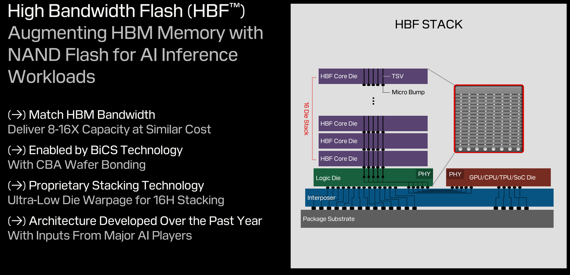
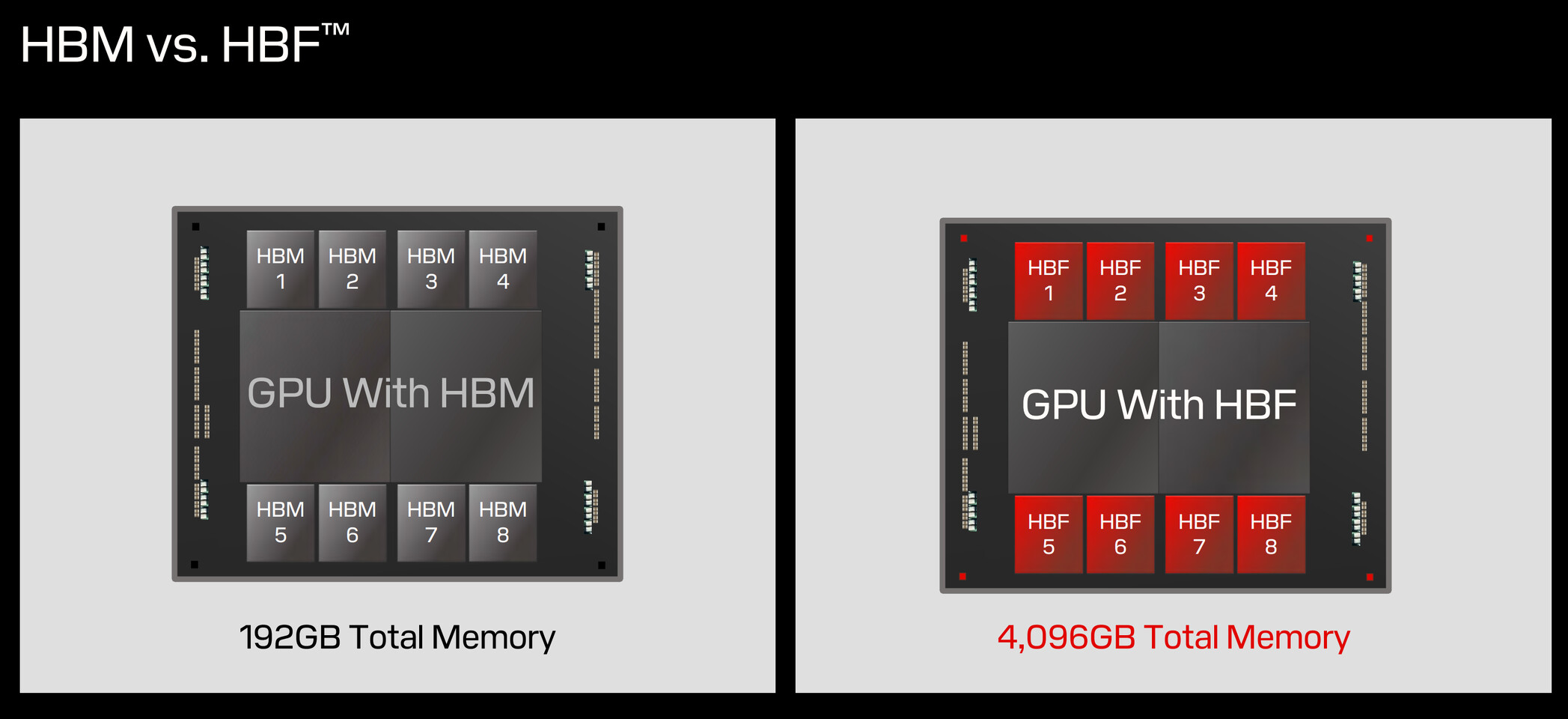
Sandisk Forms HBF Advisory Board for High-Bandwidth Flash Memory Development

Sandisk Corporation today announced the formation of a Technical Advisory Board to guide the development and strategy of its groundbreaking High Bandwidth Flash (HBF) memory technology. The board includes industry experts and senior technical leaders from both within and outside the company. Appointed today, Professor David Patterson and Raja Koduri will provide strategic guidance, technical insight, market perspective, and shape open standards as Sandisk prepares to launch HBF.

"We're honored to have two distinguished computer architecture experts join our Technical Advisory Board," said Alper Ilkbahar, Executive Vice President, Chief Technology Officer, and HBF Technical Advisory Board member at Sandisk. "Their collective experience and strategic counsel will be instrumental in shaping HBF as the future memory standard for the AI industry, and affirming we not only meet but exceed the expectations of our customers and partners."

Next‑Gen HBM4 to HBM8: Toward Multi‑Terabyte Memory on 15,000 W Accelerators

In a joint briefing this week, KAIST's Memory Systems Laboratory and TERA's Interconnection and Packaging group presented a forward-looking roadmap for High Bandwidth Memory (HBM) standards and the accelerator platforms that will employ them. Shared via Wccftech and VideoCardz, the outline covers five successive generations, from HBM4 to HBM8, each promising substantial gains in capacity, bandwidth, and packaging sophistication. First up is HBM4, targeted for a 2026 rollout in AI GPUs and data center accelerators. It will deliver approximately 2 TB/s per stack at an 8 Gbps pin rate over a 2,048-bit interface. Die stacks will reach 12 to 16 layers, yielding 36-48 GB per package with a 75 W power envelope. NVIDIA's upcoming Rubin series and AMD's Instinct MI500 cards are slated to employ HBM4, with Rubin Ultra doubling the number of memory stacks from eight to sixteen and AMD targeting up to 432 GB per device.

Looking to 2029, HBM5 maintains an 8 Gbps speed but doubles the I/O lanes to 4,096 bits, boosting throughput to 4 TB/s per stack. Power rises to 100 W and capacity scales to 80 GB using 16‑high stacks of 40 Gb dies. NVIDIA's tentative Feynman accelerator is expected to be the first HBM5 adopter, packing 400-500 GB of memory into a multi-die package and drawing more than 4,400 W of total power. By 2032, HBM6 will double pin speeds to 16 Gbps and increase bandwidth to 8 TB/s over 4,096 lanes. Stack heights can grow to 20 layers, supporting up to 120 GB per stack at 120 W. Immersion cooling and bumpless copper-copper bonding will become the norm. The roadmap then predicts HBM7 in 2035, which includes 24 Gbps speeds, 8,192-bit interfaces, 24 TB/s throughput, and up to 192 GB per stack at 160 W. NVIDIA is preparing a 15,360 W accelerator to accommodate this monstrous memory.

SanDisk Develops HBM Killer: High-Bandwidth Flash (HBF) Allows 4 TB of VRAM for AI GPUs

During its first post-Western Digital spinoff investor day, SanDisk showed something it has been working on to tackle the AI sector. High-bandwidth flash (HBF) is a new memory architecture that combines 3D NAND flash storage with bandwidth capabilities comparable to high-bandwidth memory (HBM). The HBF design stacks 16 3D NAND BiCS8 dies using through-silicon vias, with a logic layer enabling parallel access to memory sub-arrays. This configuration achieves 8 to 16 times greater capacity per stack than current HBM implementations. A system using eight HBF stacks can provide 4 TB of VRAM to store large AI models like GPT-4 directly on GPU hardware. The architecture breaks from conventional NAND design by implementing independently accessible memory sub-arrays, moving beyond traditional multi-plane approaches. While HBF surpasses HBM's capacity specifications, it maintains higher latency than DRAM, limiting its application to specific workloads.

SanDisk has not disclosed its solution for NAND's inherent write endurance limitations, though using pSLC NAND makes it possible to balance durability and cost. The bandwidth of HBF is also unknown, as the company hasn't put out details yet. SanDisk Memory Technology Chief Alper Ilkbahar confirmed the technology targets read-intensive AI inference tasks rather than latency-sensitive applications. The company is developing HBF as an open standard, incorporating mechanical and electrical interfaces similar to HBM to simplify integration. Some challenges remain, including NAND's block-level addressing limitations and writing endurance constraints. While these factors make HBF unsuitable for gaming applications, the technology's high capacity and throughput characteristics align with AI model storage and inference requirements. SanDisk has announced plans for three generations of HBF development, indicating a long-term commitment to the technology.
Return to Keyword Browsing
Aug 2nd, 2025 03:09 CDT change timezone

New Forum Posts

Popular Reviews

TPU on YouTube

Controversial News Posts