News Posts matching #Intel 20A

Return to Keyword Browsing

Intel to Tease Core Ultra "Arrow Lake" at Computex?

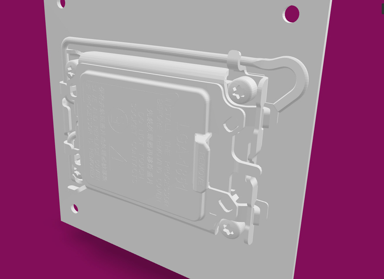
Intel is rumored to be preparing to tease its Core Ultra 2-series "Arrow Lake" processor at the 2024 Computex, which gets underway this June. The series itself isn't expected to launch before Q4-2024, but Computex is the only major global event between June and January for Intel to unveil or tease its next-generation processor, so here we are. At this point we don't know which exact platform of "Arrow Lake" Intel is planning to tease—whether these are the mobile variants, or the Socket LGA1851 desktop "Arrow Lake-S." An unveiling of the latter would almost definitely entail PC motherboard vendors being allowed to show off their first compatible motherboards at Computex—the perfect platform for them to do so.

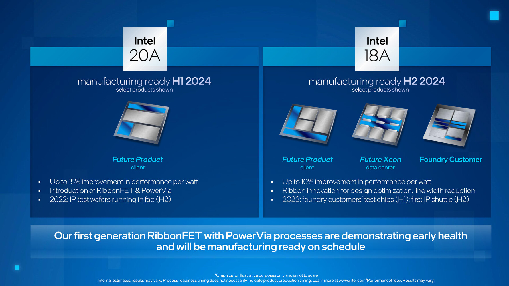
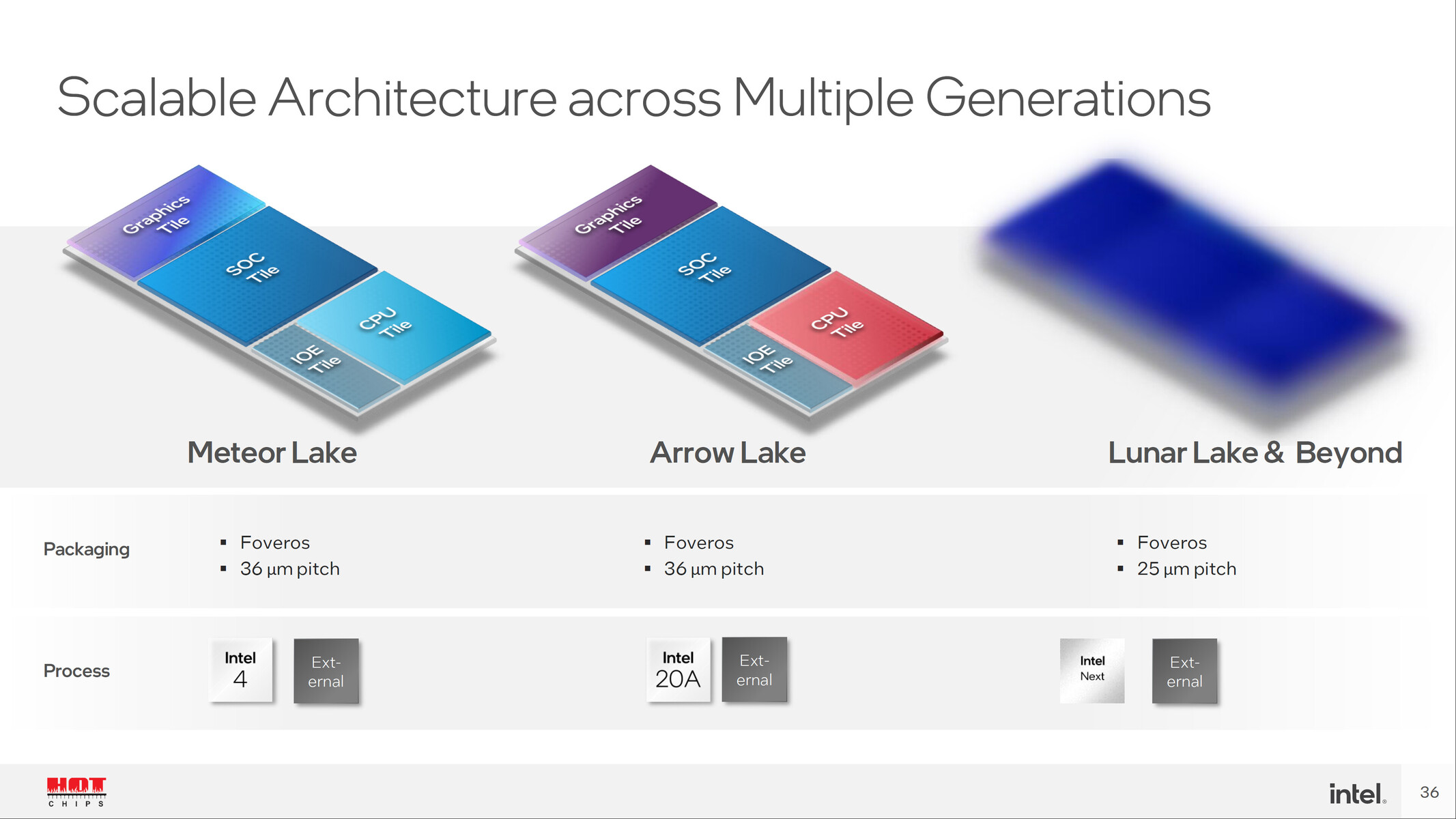
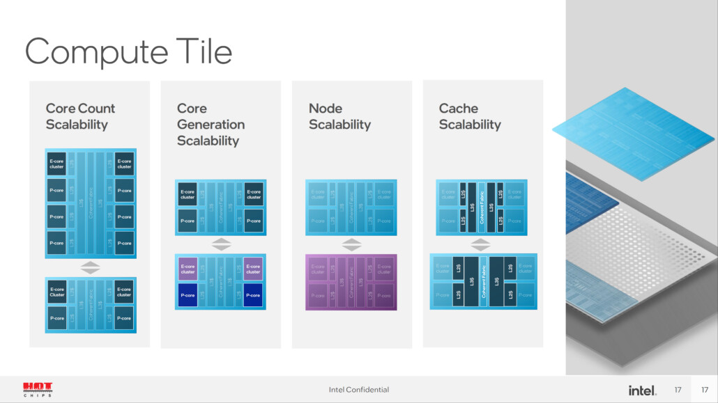
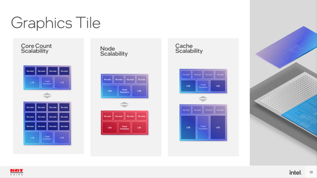
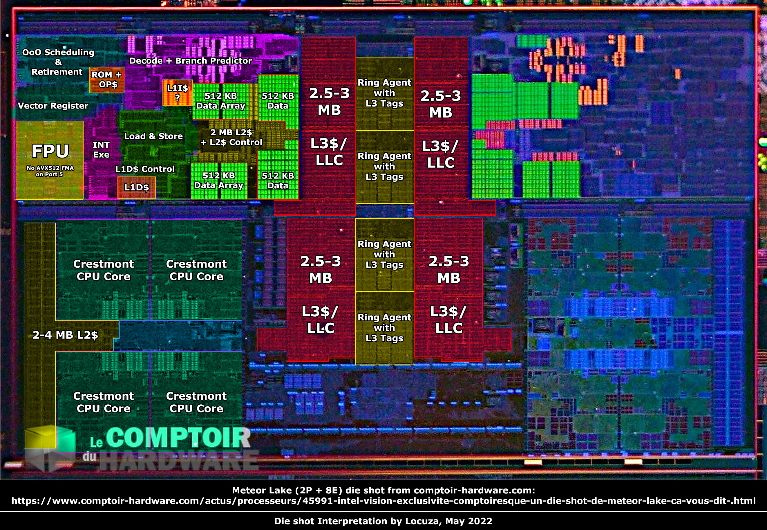
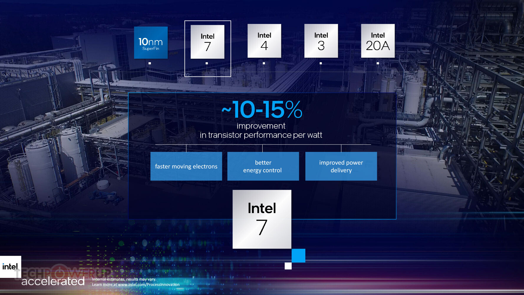
The Core Ultra "Arrow Lake" retains a Foveros Tiled (chiplet) construction of "Meteor Lake," but with advancements to the chip's Compute tile, which is built on the Intel 20A foundry node, and rocks new "Lion Cove" P-cores and "Skymont" E-cores; an updated I/O tile, and an iGPU based on the updated Xe-LPG+ graphics architecture. Since the processor now serves practically all PCH functions, the mobile "Arrow Lake" is a single-chip solution, whereas the desktop "Arrow Lake-S" is expected to remain 2-chip. There will be more I/O from the CPU, though, which is why the socket has 151 more pins than the LGA1700.

Samsung Foundry Renames 3 nm Process to 2 nm Amid Competition with Intel

In a move that could intensify competition with Intel in the cutting-edge chip manufacturing space, Samsung Foundry has reportedly decided to rebrand its second-generation 3 nm-class fabrication technology, previously known as SF3, to a 2 nm-class manufacturing process called SF2. According to reports from ZDNet, the renaming of Samsung's SF3 to SF2 is likely an attempt by the South Korean tech giant to simplify its process nomenclature and better compete against Intel Foundry, at least visually. Intel is set to roll out its Intel 20A production node, a 2 nm-class technology, later this year. The reports suggest that Samsung has already notified its customers about the changes in its roadmap and the renaming of SF3 to SF2. Significantly, the company has reportedly gone as far as re-signing contracts with customers initially intended to use the SF3 production node.

"We were informed by Samsung Electronics that the 2nd generation 3 nm [name] is being changed to 2 nm," an unnamed source noted to ZDNet. "We had contracted Samsung Foundry for the 2nd generation 3 nm production last year, but we recently revised the contract to change the name to 2 nm." Despite the name change, Samsung's SF3, now called SF2, has not undergone any actual process technology alterations. This suggests that the renaming is primarily a marketing move, as using a different process technology would require customers to rework their chip designs entirely. Samsung intends to start manufacturing chips based on the newly named SF2 process in the second half of 2024. The SF2 technology, which employs gate-all-around (GAA) transistors that Samsung brands as Multi-Bridge-Channel Field Effect Transistors (MBCFET), does not feature a backside power delivery network (BSPDN), a significant advantage of Intel's 20A process. Samsung Foundry has not officially confirmed the renaming.

Intel Core Ultra 2-series "Arrow Lake-S" Desktop Features 4 Xe-core iGPU, No Island Cores

Over the weekend, there have been a series of leaks from sources such as Golden Pig Upgrade, and High Yield YT, surrounding Intel's next-generation desktop processor, the Core Ultra 2-series "Arrow Lake-S." The lineup is likely to continue the new client processor naming scheme Intel introduced with the Core Ultra 1-series "Meteor Lake" on the mobile platform. "Arrow Lake-S" is rumored to debut the new Socket LGA1851, which retains cooler-compatibility with LGA1700. Although Intel has nucleated all I/O functions of the traditional PCH to "Meteor Lake," making it a single-chip solution on the mobile platform; and although the mobile "Arrow Lake" will continue to be single-chip; the desktop "Arrow Lake-S" will be a 2-chip solution. This is mainly because the desktop platform demands a lot more PCIe lanes, for a larger number of NVMe storage devices, or high bandwidth devices such as Thunderbolt and USB4 hubs, etc.

Another key finding in this latest series of leaks, is that unlike "Meteor Lake," the desktop "Arrow Lake-S" will do away with low-power island E-cores located in the SoC tile of the processor. All CPU cores are located in the Compute tile, which is expected to be built in the Intel 20A foundry node—the company's first node to implement GAAFETs (nanosheets), with backside power delivery; as well as an advanced 2nd generation EUV lithography. Intel's 1st Gen EUV is used on the current FinFET-based Intel 4 and Intel 3 foundry nodes.

Report: Intel Seeks $2 Billion in Funding for Ireland Fab 34 Expansion

According to a Bloomberg report, Intel is seeking to raise at least $2 billion in equity funding from investors for expanding its fabrication facility in Leixlip, Ireland, known as Fab 34. The chipmaker has hired an advisor to find potential investors interested in providing capital for the project. Fab 34 is currently Intel's only chip plant in Europe that uses cutting-edge extreme ultraviolet (EUV) lithography. It produces processors on the Intel 4 process node, including compute tiles for Meteor Lake client CPUs and expected future Xeon data center chips. While $2 billion alone cannot finance the construction of an entirely new fab today, it can support meaningful expansion or upgrades of existing capacity. Intel likely aims to grow Fab 34's output and/or transition it to more advanced 3 nm-class technologies like Intel 3, Intel 20A, or Intel 18A.

Expanding production aligns with Intel's needs for its own products and its Intel Foundry Services business, providing contract manufacturing. Intel previously secured a $15 billion investment from Brookfield Infrastructure for its Arizona fabs in exchange for a 49% stake, demonstrating the company's willingness to partner to raise capital for manufacturing projects. The Brookfield deal also set a precedent of using outside financing to supplement Intel's own spending budget. It provided $15 billion in effectively free cash flow Intel can redirect to other priorities like new fabs without increasing debt. Intel's latest fundraising efforts for the Ireland site follow a similar equity investment model that leverages outside capital to support its manufacturing expansion plans. Acquiring High-NA EUV machinery for manufacturing is costly, as these machines can reach up to $380 million alone.

Intel Unveils "Arrow Lake" for Desktops, "Lunar Lake" for Mobile, Coming This Year

Intel in its 2024 International CES presentation, unveiled its two new upcoming client microarchitectures, "Arrow Lake" and "Lunar Lake." Michelle Johnston Holthaus, EVP and GM of Intel's client computing group (CCG), in her keynote address, held up a next-generation Core Ultra "Lunar Lake" chip. This is the Lunar Lake-MX package, with MOP (memory on package). You have a Foveros base tile resembling "Meteor Lake," with on-package LPDDR5x memory stacks. With "Lunar Lake," Intel is reorganizing components across its various Foveros tiles—the Compute and Graphics tiles are combined into a single tile built on an Intel foundry node that's possibly the Intel 20A (we have no confirmation); and a smaller SoC tile that has all of the components of the current "Meteor Lake" SoC tile, and is possibly built on a TSMC node, such as N3.

"Lunar Lake" will pick up the mantle from "Meteor Lake" in the U-segment and H-segment (that's ultraportables, and thin-and-light), when it comes out later this year (we predict in the second half of 2024), with Core Ultra 2-series branding. Intel also referenced "Arrow Lake," which could finally bring light to the sluggish pace of development in its desktop segment. When it comes out later this year, "Arrow Lake" will debut Socket LGA1851, "Arrow Lake" will bring the AI Boost NPU to the desktop, along with Arc Xe-LPG integrated graphics. The biggest upgrade of course will be its new Compute tile, with its "Lion Cove" P-cores, and "Skymont" E-cores, that possibly offer a large IPC uplift over the current combination of "Raptor Cove" and "Gracemont" cores on the "Raptor Lake" silicon. It's also possible that Intel will try to bring "Meteor Lake" with its 6P+8E Compute tile, Xe-LPG iGPU, and NPU, to the LGA1851 socket, as part of some mid-range processor models. 2024 will see a Intel desktop processor based on a new architecture, which is the big takeaway here.

Intel's Arizona Expansion Marks Construction Milestone

Marking a milestone in Intel's ongoing manufacturing expansion in Arizona, the company today announced that the initial portion of the cleanroom is "weather tight" and the "blow down" phase has begun at the company's two new leading-edge chip factories on its Ocotillo campus in Chandler, Arizona. This milestone underscores Intel's dedication to advancing its presence in the state and fostering technological innovation.

"Our commitment to Arizona runs deep, and as we expand our operations, we remain dedicated to addressing the growing demand for semiconductors and helping the United States regain its leadership position in this vital industry. This milestone represents the result of great teamwork, proficient teams and exceptional craftsmanship of the tradespeople, and it's thanks to their hard work that we've made such significant progress on our site while keeping our culture of caring and the safety of all as our top priority." -Dan Doron, Intel vice president and general manager of Fab Construction Enterprise

Intel LGA-1851 "Arrow Lake" Socket Detailed

Thanks to the 3D renders and technical drawings obtained by Igor's Lab, we have insights into the structure of Intel's next-generation LGA-1851 socket for Arrow Lake processors. Scheduled to arrive in mid-2024, the LGA-1851 socket was originally intended for Meteor Lake-S desktop processors. However, the socket is now awaiting Arrow Lake since Meteor Lake is now a mobile-only processor generation. The first notable thing about LGA-1851 is that it will directly connect a dedicated PCIe 5.0 x4 interface to the CPU, besides the x16 lanes going to the GPU. This results in native support for high-speed PCIe 5.0 NVMe SSDs that can achieve speeds of over 12 GB/s in both read and write workloads.

Intel Arrow Lake-S will be available with eight P-cores and 16 E-cores in SKUs with different combinations of the two. The accompanying 800 series chipset includes Z890, B860, and H810 models, with an evident absence of H870 SKU. There will be W880 and Q870 workstation-grade chipsets as well. It is worth pointing out that Arrow Lake will enable DRAM capacities of up to 48 GB per DIMM at 6400 MT/s. We expect to hear more about Arrow Lake-S as we near the 2024 launch date and we get to see the Intel 20A node being used in client products. Below, you can see the technical drawings of the Independent Loading Mechanism (ILM) and chipset 3D models.

Intel Demoes Core "Lunar Lake" Processor from Two Generations Ahead

Intel at the 2023 InnovatiON event surprised audiences with a live demo of a reference notebook powered by a Core "Lunar Lake" processor. What's surprising about this is that "Lunar Lake" won't come out until 2025 (at least), and succeeds not just the upcoming "Meteor Lake" architecture, but also its succeeding "Arrow Lake," which debuts in 2024. Intel is expected to debut "Meteor Lake" some time later this year. What's also surprising is that Intel has proven that the Intel 18A foundry node works. The Compute tile of "Lunar Lake" is expected to be based on Intel 18A, which is four generations ahead of the current Intel 7, which will be succeeded by Intel 4, Intel 3, and Intel 20A along the way.

The demo focused on the generative AI capabilities of Intel's third generation NPU, the hardware backend of AI Boost. Using a local session of a tool similar to Stable Diffusion, the processor was made to generate the image of a giraffe wearing a hat; and a GPT program was made to pen the lyrics of a song in the genre of Taylor Swift from scratch. Both tasks were completed on stage using the chip's NPU, and in timeframes you'd normally expect from discrete AI accelerators or cloud-based services.

Intel Reports Second-Quarter 2023 Financial Results, Foundry Services Business up

Intel Corporation today reported second-quarter 2023 financial results. "Our Q2 results exceeded the high end of our guidance as we continue to execute on our strategic priorities, including building momentum with our foundry business and delivering on our product and process roadmaps," said Pat Gelsinger, Intel CEO. "We are also well-positioned to capitalize on the significant growth across the AI continuum by championing an open ecosystem and silicon solutions that optimize performance, cost and security to democratize AI from cloud to enterprise, edge and client."

David Zinsner, Intel CFO, said, "Strong execution, including progress towards our $3 billion in cost savings in 2023, contributed to the upside in the quarter. We remain focused on operational efficiencies and our Smart Capital strategy to support sustainable growth and financial discipline as we improve our margins and cash generation and drive shareholder value." In the second quarter, the company generated $2.8 billion in cash from operations and paid dividends of $0.5 billion.

Intel, Ericsson Expand Collaboration to Advance Next-Gen Optimized 5G Infrastructure

Today, Intel announced a strategic collaboration agreement with Ericsson to utilize Intel's 18A process and manufacturing technology for Ericsson's future next-generation optimized 5G infrastructure. As part of the agreement, Intel will manufacture custom 5G SoCs (system-on-chip) for Ericsson to create highly differentiated leadership products for future 5G infrastructure. Additionally, the companies will expand their collaboration to optimize 4th Gen Intel Xeon Scalable processors with Intel vRAN Boost for Ericsson's Cloud RAN (radio access network) solutions to help communications service providers increase network capacity and energy efficiency while gaining greater flexibility and scalability.

"As our work together evolves, this is a significant milestone with Ericsson to partner broadly on their next-generation optimized 5G infrastructure. This agreement exemplifies our shared vision to innovate and transform network connectivity, and it reinforces the growing customer confidence in our process and manufacturing technology," said Sachin Katti, senior vice president and general manager of the Network and Edge group at Intel. "We look forward to working together with Ericsson, an industry leader, to build networks that are open, reliable and ready for the future."

With PowerVia, Intel Achieves a Chipmaking Breakthrough

Intel is about to turn chipmaking upside down with PowerVia, a new approach to delivering power that required a radical rethink to both how chips are made and how they are tested. For all the modern history of computer chips, they've been built like pizzas—from the bottom up, in layers. In the case of chips, you start with the tiniest features, the transistors, and then you build up increasingly less-tiny layers of wires that connect the transistors and different parts of the chip (these are called interconnects). Included among those top layers are the wires that bring in the power that makes the chip go.

When the chip is done, you flip it over, enclose it in packaging that provides connections to the outer world, and you're ready to put it in a computer. Unfortunately, this approach is running into problems. As they get smaller and denser, the layers that share interconnects and power connections have become an increasingly chaotic web that hinders the overall performance of each chip. Once an afterthought, "now they have a huge impact," says Ben Sell, vice president of Technology Development at Intel and part of the team that brought PowerVia to fruition. In short, power and signals fade, requiring workarounds or simply dumping more power in.

Intel to Demonstrate PowerVia on E-Core Processor Built with Intel 4 Node

At VLSI Symposium 2023, scheduled to take place between June 11-16, Intel is set to demonstrate its PowerVia technology working efficiently on an E-Core chip built using the Intel 4 node. Conventional chips have power and signal interconnects distributed across multiple metal layers. PowerVia, on the other hand, dedicates specific layers for power delivery, effectively separating them from the signal routing layers. This approach allows for vertical power delivery through a set of power-specific Through-Silicon Vias (TSVs) or PowerVias, which are essentially vertical connections between the top and bottom surfaces of the chip. By delivering power directly from the backside of the chip, PowerVia reduces power supply noise and resistive losses, optimizing power distribution and improving overall energy efficiency. PowerVia is set to make a debut in 2024 with Intel 20A node.

For VLSI Symposium 2023 talk, the company has prepared a paper that highlights a design made using Intel 4 technology and implements E-Cores only in a test chip. The document states: "PowerVia Technology is a novel innovation to extend Process Scaling by having Power Delivery on the backside. This paper presents the pre and post silicon findings from implementing an Intel E-Core in PowerVia Technology. PowerVia enabled standard cell utilization of greater than 90 percent in large areas of the core while showing greater than 5 percent frequency benefit in silicon due reduced IR drop. Successful Post silicon debug is demonstrated with slightly higher but acceptable throughput times. The thermal characteristics of the PowerVia testchip is inline with higher power densities expected from logic scaling."

Intel Reports First-Quarter 2023 Financial Results: Client and Server Businesses Down 38-39% Each

Intel Corporation today reported first-quarter 2023 financial results. "We delivered solid first-quarter results, representing steady progress with our transformation," said Pat Gelsinger, Intel CEO. "We hit key execution milestones in our data center roadmap and demonstrated the health of the process technology underpinning it. While we remain cautious on the macroeconomic outlook, we are focused on what we can control as we deliver on IDM 2.0: driving consistent execution across process and product roadmaps and advancing our foundry business to best position us to capitalize on the $1 trillion market opportunity ahead."

David Zinsner, Intel CFO, said, "We exceeded our first-quarter expectations on the top and bottom line, and continued to be disciplined on expense management as part of our commitment to drive efficiencies and cost savings. At the same time, we are prioritizing the investments needed to advance our strategy and establish an internal foundry model, one of the most consequential steps we are taking to deliver on IDM 2.0."

Intel 20A and 18A Foundry Nodes Complete Development Phase, On Track for 2024 Manufacturing

Intel Foundry Services, the in-house semiconductor foundry of Intel, announced that its 2 nm-class Intel 20A and 1.8 nm-class Intel 18A foundry nodes have completed development, and are on course for mass-producing chips on their roadmap dates. Chips are expected to begin mass-production on the Intel 20A node in the first half of 2024, while those on the Intel 18A node are expected to begin in the second half of 2024. The completion of the development phase means that Intel has finalized the specifications and performance/power targets of the nodes, the tools and software required to make the chips, and can now begin ordering them to build the nodes. Intel has been testing these nodes through 2022, and with the specs being finalized, chip-designers can accordingly wrap up development of their products to align with what these nodes have to offer.

Intel 20A (or 20-angstrom, or 2 nm) node introduces gates-all-around (GAA) RibbonFET transistors with PowerVIAs (an interconnect innovation that contributes to transistor densities). The Intel 20A node is claimed to offer a 15% performance/Watt gain over its predecessor, the Intel 3 node (FinFET EUV, 3 nm-class), which by itself offers an 18% performance/Watt gain over Intel 4 (20% perf/Watt gain over the current Intel 7 node), the node that is entering mass-production very soon. The Intel 18A node is a further refinement of Intel 20A, and introduces a design improvement to the RibbonFET that increases transistor density at scale, and a claimed 10% performance/Watt improvement over Intel 20A.

Intel Reports Fourth-Quarter and Full-Year 2022 Financial Results, Largest Loss in Years

Intel Corporation today reported fourth-quarter and full-year 2022 financial results. The company also announced that its board of directors has declared a quarterly dividend of $0.365 per share on the company's common stock, which will be payable on March 1, 2023, to shareholders of record as of February 7, 2023.

"Despite the economic and market headwinds, we continued to make good progress on our strategic transformation in Q4, including advancing our product roadmap and improving our operational structure and processes to drive efficiencies while delivering at the low-end of our guided range," said Pat Gelsinger, Intel CEO. "In 2023, we will continue to navigate the short-term challenges while striving to meet our long-term commitments, including delivering leadership products anchored on open and secure platforms, powered by at-scale manufacturing and supercharged by our incredible team."

Intel's Next-Gen Desktop Platform Intros Socket LGA1851, "Meteor Lake-S" to Feature 6P+16E Core Counts

Keeping up with the cadence of two generations of desktop processors per socket, Intel will turn the page of the current LGA1700, with the introduction of the new Socket LGA1851. The processor package will likely have the same dimensions as LGA1700, and the two sockets may share cooler compatibility. The first processor microarchitecture to debut on LGA1851 will be the 14th Gen Core "Meteor Lake-S." These chips will feature a generationally lower CPU core-count compared to "Raptor Lake," but significantly bump the IPC on both the P-cores and E-cores.

"Raptor Lake" is Intel's final monolithic silicon client processor before the company pivots to chiplets built on various foundry nodes, as part of its IDM 2.0 strategy. The client-desktop version of "Meteor Lake," dubbed "Meteor Lake-S," will have a maximum CPU core configuration of 6P+16E (that's 6 performance cores with 16 efficiency cores). The chip has 6 "Redwood Cove" P-cores, and 16 "Crestmont" E-cores. Both of these are expected to receive IPC uplifts, such that the processor will end up faster (and hopefully more efficient) than the top "Raptor Lake-S" part. Particularly, it should be able to overcome the deficit of 2 P-cores.

Intel Reports Third-Quarter 2022 Financial Results

Intel Corporation today reported third-quarter 2022 financial results. "Despite the worsening economic conditions, we delivered solid results and made significant progress with our product and process execution during the quarter," said Pat Gelsinger, Intel CEO. "To position ourselves for this business cycle, we are aggressively addressing costs and driving efficiencies across the business to accelerate our IDM 2.0 flywheel for the digital future."

"As we usher in the next phase of IDM 2.0, we are focused on embracing an internal foundry model to allow our manufacturing group and business units to be more agile, make better decisions and establish a leadership cost structure," said David Zinsner, Intel CFO. "We remain committed to the strategy and long-term financial model communicated at our Investor Meeting."

US Institutes GAA-FET Technology EDA Software Ban on China, Stalling sub-3nm Nodes

The US Government has instituted a ban on supply of GAA-FET EDA software to China (the Chinese government and companies in China). Humans can no longer design every single circuit on chips with tens of billions of transistors, and so EDA (electronics design automation) software is used to micromanage design based broadly on what chip architects want. Synopsys, Cadence, and Siemens are major EDA software suppliers. Intel is rumored to use an in-house EDA software that it doesn't sell, although this could change with the company roping in third-party foundries, such as TSMC, for cutting-edge logic chips (which will need the software to make sense of Intel's designs).

GAA or "gates-all-around" technology is vital to building transistors in the 3 nm and 2 nm silicon fabrication nodes. Samsung is already using GAA for its 3 nm node, while TSMC intends to use it with its 2N (2 nm) node. Intel is expected to use it with its Intel 20A (20 angstrom, or 2 nanometers) node. Both Intel and TSMC will debut nodes powered by GAAFETs for mass-production in 2024. The US Government has already banned the sales of EUV lithography machines to China, as well as machines fabricating 3D NAND flash chips with greater than 128 layers or 14 nm. In the past, technology embargoes have totally stopped China from copying or reverse-engineering western tech, or luring Taiwanese engineers armed with industry secrets away on the promise of wealth and a comfortable life in the Mainland.

Intel "Meteor Lake" 2P+8E Silicon Annotated

Le Comptoir du Hardware scored a die-shot of a 2P+8E core variant of the "Meteor Lake" compute tile, and Locuza annotated it. "Meteor Lake" will be Intel's first processor to implement the company's IDM 2.0 strategy to the fullest. The processor is a multi-chip module of various tiles (chiplets), each with a certain function, sitting on die made on a silicon fabrication node most suitable to that function. Under this strategy, for example, if Intel's chip-designers calculate that the iGPU will be the most power-hungry component on the processor, followed by the CPU cores, the graphics tile will be built on a more advanced process than the compute tile. Intel's "Meteor Lake" and "Arrow Lake" processors will implement chiplets built on the Intel 4, TSMC N3, and Intel 20A fabrication nodes, each with unique power and transistor-density characteristics. Learn more about the "Meteor Lake" MCM in our older article.

The 2P+8E (2 performance cores + 8 efficiency cores) compute tile is one among many variants of compute tiles Intel will develop for the various SKUs making up the next-generation Core mobile processor series. The die is annotated with the two large "Redwood Cove" P-cores and their cache slices taking up about 35% of the die area; and the two "Crestmount" E-core clusters (each with 4 E-cores), and their cache slices, taking up the rest. The two P-cores and two E-core clusters are interconnected by a Ring Bus, and share an L3 cache. The size of each L3 cache slice is either 2.5 MB or 3 MB. At 2.5 MB, the total L3 cache will be 10 MB, and at 3 MB, it will be 12 MB. As with all past generations, the L3 cache is fully accessible by all CPU cores in the compute tile.

Intel Makes Jilted Reference to Apple in its Internal "Arrow Lake" Slide

Intel is designing a "Halo" SKU of a future generation of mobile processors with a goal to match Apple's in-house silicon of the time. Slated for tape-out some time in 2023, with mass-production expected in 2024, the 15th Generation Core "Arrow Lake-P Halo" processor is being designed specifically to compete with Apple's "premium 14-inch laptop" (presumably the MacBook Pro) that the company could have around 2024, based on an in-house Apple silicon. This is to essentially tell its notebook partners that they will have an SoC capable of making their devices in the class truly competitive. Apple relies on a highly scaled out Arm-based SoC based on in-house IP blocks, with a software that's closely optimized for it. Intel's effort appears to chase down its performance and efficiency.

The Core "Arrow Lake" microarchitecture succeeds the 14th Gen "Meteor Lake." It is a multi-chip module (MCM) of three distinct dies built on different fabrication nodes, in line with the company's IDM 2.0 strategy. These nodes are Intel 4 (comparable to TSMC N7 or N6), Intel 20A (comparable to TSMC N5), and an "external" 3 nm-class node that's just the TSMC N3. The compute tile, or the die which houses the CPU cores, combines a hybrid CPU setup of 6 P-cores, and 8 E-cores. The performance cores are likely successors of the "Redwood Cove" P-cores powering the "Meteor Lake" compute tiles. Intel appears to be using one kind of E-cores across two generations (eg: Gracemont across Alder Lake and Raptor Lake). If this is any indication, Arrow Lake could continue to use "Crestmont" E-cores. Things get interesting with the Graphics tile.

Intel "Meteor Lake" and "Arrow Lake" Use GPU Chiplets

Intel's upcoming "Meteor Lake" and "Arrow Lake" client mobile processors introduce an interesting twist to the chiplet concept. Earlier represented in vague-looking IP blocks, new artistic impressions of the chip put out by Intel shed light on a 3-die approach not unlike the Ryzen "Vermeer" MCM that has up to two CPU core dies (CCDs) talking to a cIOD (client IO die), which handles all the SoC connectivity; Intel's design has one major difference, and that's integrated graphics. Apparently, Intel's MCM uses a GPU die sitting next to the CPU core die, and the I/O (SoC) die. Intel likes to call its chiplets "tiles," and so we'll go with that.

The Graphics tile, CPU tile, and the SoC or I/O tile, are built on three different silicon fabrication process nodes based on the degree of need for the newer process node. The nodes used are Intel 4 (optically 7 nm EUV, but with characteristics of a 5 nm-class node); Intel 20A (characteristics of 2 nm), and external TSMC N3 (3 nm) node. At this point we don't know which tile gets what. From the looks of it, the CPU tile has a hybrid CPU core architecture made up of "Redwood Cove" P-cores, and "Crestmont" E-core clusters.

Intel Updates Technology Roadmap with Data Center Processors and Game Streaming Service

At Intel's 2022 Investor Meeting, Chief Executive Officer Pat Gelsinger and Intel's business leaders outlined key elements of the company's strategy and path for long-term growth. Intel's long-term plans will capitalize on transformative growth during an era of unprecedented demand for semiconductors. Among the presentations, Intel announced product roadmaps across its major business units and key execution milestones, including: Accelerated Computing Systems and Graphics, Intel Foundry Services, Software and Advanced Technology, Network and Edge, Technology Development, More: For more from Intel's Investor Meeting 2022, including the presentations and news, please visit the Intel Newsroom and Intel.com's Investor Meeting site.

Intel Reports Third-Quarter 2021 Financial Results

Intel Corporation today reported third-quarter 2021 financial results. "Q3 shone an even greater spotlight on the global demand for semiconductors, where Intel has the unique breadth and scale to lead. Our focus on execution continued as we started delivering on our IDM 2.0 commitments. We broke ground on new fabs, shared our accelerated path to regain process performance leadership, and unveiled our most dramatic architectural innovations in a decade. We also announced major customer wins across every part of our business," said Pat Gelsinger, Intel CEO. "We are still in the early stages of our journey, but I see the enormous opportunity ahead, and I couldn't be prouder of the progress we are making towards that opportunity."

In the third quarter, the company generated $9.9 billion in cash from operations and paid dividends of $1.4 billion. Intel CFO George Davis announced plans to retire from Intel in May 2022. He will continue to serve in his current role while Intel conducts a search for a new CFO and until his successor is appointed. Third-quarter revenue was led by strong recovery in the Enterprise portion of DCG and in IOTG, which saw higher demand amid recovery from the economic impacts of COVID-19. The Client Computing Group (CCG) was down due to lower notebook volumes due to industry-wide component shortages, and on lower adjacent revenue, partially offset by higher average selling prices (ASPs) and strength in desktop.

Intel Rebadges 10nm Enhanced SuperFin Node as "Intel 7," Invents Other Creative Node Names

Intel, in a move comparable to its competitors' Performance Rating system from the 1990s, has invented a new naming scheme for its in-house foundry nodes to claim technological parity with contemporaries such as TSMC and Samsung, that are well into the sub-10 nm class. Back in the i586 era, when Intel's competitors such as AMD and Cyrix, couldn't keep up with its clock-speeds yet found their chips to be somewhat competitive, they invented the PR (processor rating) system, with a logical number attempting to denote parity with an Intel processor's clock-speed. For example, a PR400 processor rating meant that the chip rivaled a Pentium II 400 MHz (which it mostly didn't). The last that the PR system made sense was with the final generation of single-core performance chips, Pentium 4 and Athlon XP, beyond which, the introduction of multi-core obfuscated the PR system. A Phenom X4 9600 processor didn't mean performance on par with a rival Intel chip running at an impossible 9.60 GHz.

Intel's new foundry naming system sees its 10 nm Enhanced SuperFin node re-badge as "Intel 7." The company currently builds 11th Gen Core "Tiger Lake" processors on the 10 nm SuperFin node, and is expected to build its upcoming 12th Gen Core "Alder Lake" chips on its refinement, the 10 nm Enhanced SuperFin, which will now be referred to as "Intel 7." The company is careful to avoid using the nanometer unit next to the number, instead signaling the consumer that the node somehow offers transistor density and power characteristics comparable to a 7 nm node. Intel 7 offers a 10-15 percent performance/Watt gain over 10 nm SuperFin, and is already in volume production, with a debut within 2021 with "Alder Lake."

Intel Accelerates Packaging and Process Innovations

Intel Corporation today revealed one of the most detailed process and packaging technology roadmaps the company has ever provided, showcasing a series of foundational innovations that will power products through 2025 and beyond. In addition to announcing RibbonFET, its first new transistor architecture in more than a decade, and PowerVia, an industry-first new backside power delivery method, the company highlighted its planned swift adoption of next-generation extreme ultraviolet lithography (EUV), referred to as High Numerical Aperture (High NA) EUV. Intel is positioned to receive the first High NA EUV production tool in the industry.

"Building on Intel's unquestioned leadership in advanced packaging, we are accelerating our innovation roadmap to ensure we are on a clear path to process performance leadership by 2025," Intel CEO Pat Gelsinger said during the global "Intel Accelerated" webcast. "We are leveraging our unparalleled pipeline of innovation to deliver technology advances from the transistor up to the system level. Until the periodic table is exhausted, we will be relentless in our pursuit of Moore's Law and our path to innovate with the magic of silicon."
Return to Keyword Browsing
Apr 19th, 2024 16:14 EDT change timezone

New Forum Posts

Popular Reviews

Controversial News Posts