News Posts matching #Ivy Bridge-E

Return to Keyword Browsing

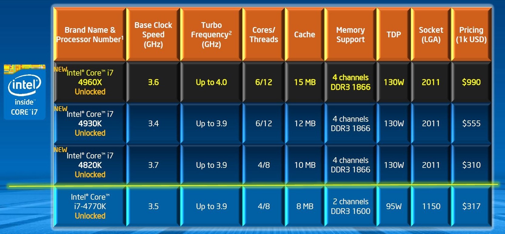
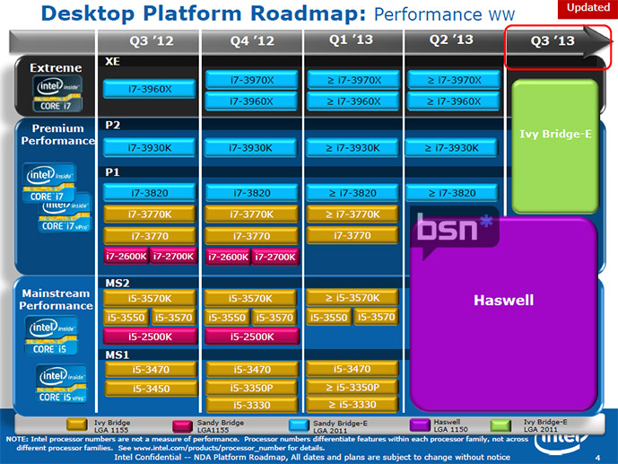
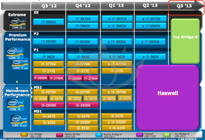
Intel Core i7 "Ivy Bridge-E" HEDT Processors Start Selling

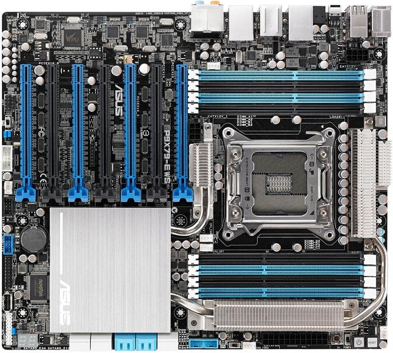
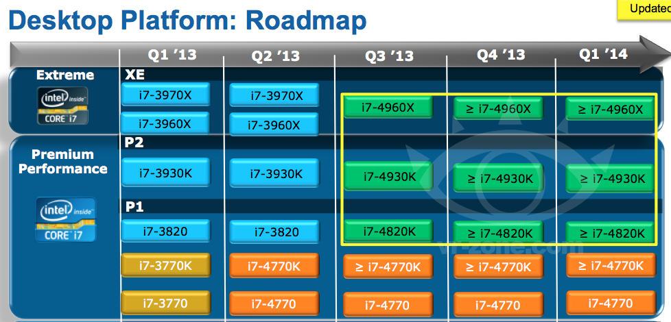
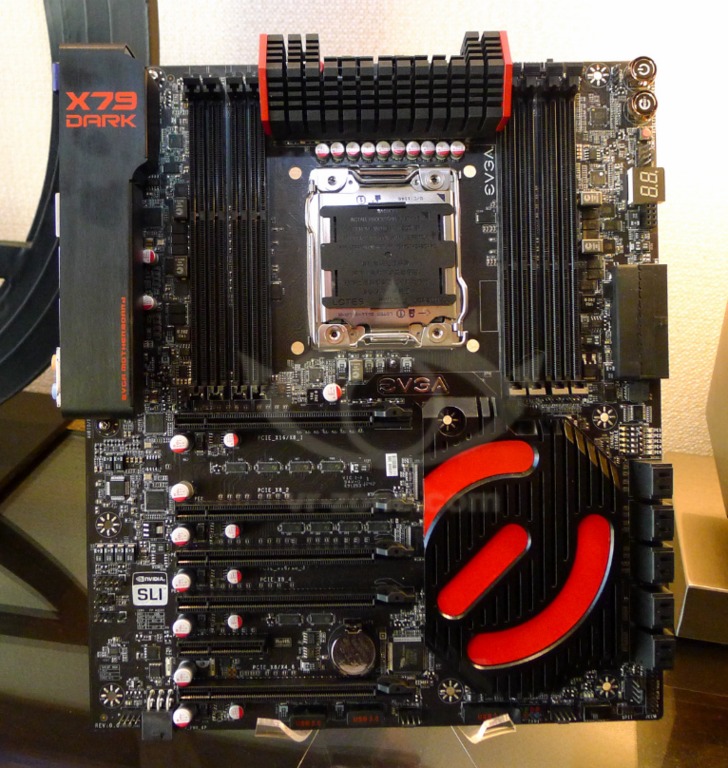
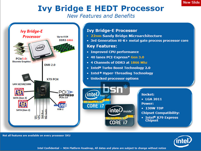
Intel made its newest Core i7 high-end desktop (HEDT) platform official with the launch of three new socket LGA2011 processors based on the swanky new 22 nm "Ivy Bridge-E" silicon. The launch includes the top-end Core i7-4960X Extreme Edition, priced at $990, followed by the Core i7-4930K at $555, and Core i7-4820K at $310. Expect a 10 percent markup across the board for these prices. Of these, the i7-4960X and i7-4930K are six-core parts, while the i7-4820K is quad-core.

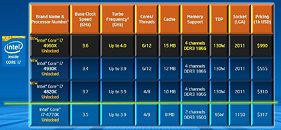
The Core i7-4960X features a CPU clock speed of 3.60 GHz, with up to 4.00 GHz Turbo Boost frequency, 15 MB of L3 cache, and HyperThreading, which enables 12 logical CPUs for the OS to deal with. The i7-4930K clocks in at 3.40 GHz, with up to 3.90 GHz Turbo Boost, 12 MB of L3 cache, and HyperThreading. The i7-4820K, at its price point, can be extremely inviting for people with their minds set on a Core i7-4770K. It features 3.70 GHz clocks with up to 3.90 GHz Turbo Boost, 10 MB of L3 cache, and HyperThreading, enabling 8 logical CPUs. All three parts feature quad-channel DDR3 integrated memory controller with native support for DDR3-1866, 48-lane PCI-Express gen 3.0 root complexes, and 130W rated TDPs.

ASUS Posts Official Ivy Bridge-E BIOS Updates for its LGA2011 Motherboards

ASUS posted official BIOS updates for its socket LGA2011 motherboards, that let them support Intel Core i7 "Ivy Bridge-E" processors. The updates can be installed either using an old LGA2011 processor, or using ASUS USB BIOS Flashback, in the absence of an older processor. For ASUS' mainline P9X79 series, "Ivy Bridge-E" support is lent by BIOS version number 4301. The P9X79 series includes P9X79 LE, P9X79, P9X79 Pro, and P9X79 Deluxe. For ROG Rampage IV Extreme and Rampage IV Gene, it's version 4401, and for ROG Rampage IV Formula, it's 4402. For TUF Sabertooth X79 it's version 4309. Get your corresponding BIOS file here.

Ivy Bridge-E Not a Cut-down 8-core, 20 MB LLC Die

Unlike Core i7 "Sandy Bridge-E," chips, which were quad-core or six-core parts cut-down from a common silicon shared with Xeon "Sandy Bridge-EP," which physically features eight cores and 20 MB of L3 cache; the upcoming Core i7 "Ivy Bridge-E" is based on a silicon that physically features just six cores, and 15 MB (or maybe 16 MB) of L3 cache. On the Core i7-4960X Extreme Edition, practically no component on the die is disabled. The Core i7-4930K features just 12 MB of L3 cache, while the Core i7-4820K features two out of six cores disabled, and just 10 MB of L3 cache.

"Ivy Bridge-E" is a variant of one of three large 22 nm dies Intel designed, based on the "Ivy Bridge" micro-architecture, next to a 10-core die with 25 MB of L3 cache, and a 12-core die with 30 MB of L3 cache. Aside from up to six cores, "Ivy Bridge-E" features a PCI-Express gen 3.0 certified root-complex (certified in way that NVIDIA would approve of), and a quad-channel (256-bit wide) DDR3 integrated memory controller, with native support for DDR3-1866. Intel's Core i7 "Ivy Bridge-E" series should launch on or before the 10th of September. Parts in the series will run on existing socket LGA2011 motherboards, with a BIOS update.

Core i7 "Ivy Bridge-E" Pricing Surfaces

With Core i7-4770K "Haswell" and Z87-based motherboard combos going for as low as $450, Intel is shaping its upcoming Core i7 "Ivy Bridge-E" HEDT platform in a way that doesn't create a big pricing gap between the two platforms, and that those with the monies for an i7-4770K + Z87 platform are sufficiently tempted to drop in a few extra coins for an HEDT platform.

To begin with, Core i7-4820K is expected to be priced at US $310, a whole $40 cheaper than the Core i7-4770K. This quad-core chip features 3.70 GHz clocks, 3.90 GHz maximum Turbo Boost, 10 MB of L3 cache, 48 PCI-Express gen 3.0 lanes, and a quad-channel memory controller; compared to the 3.60 GHz clocks, 3.90 GHz Turbo Boost, 8 MB L3 cache, 24 PCI-Express gen 3.0 lanes, and a dual-channel memory controller. To its credit, the i7-4770K features higher IPC thanks to its more advanced micro-architecture. Socket LGA2011 motherboards, such as Intel's DX79TO can be had for as low as $150. Tempting offer there.

ASUS Intros Ivy Bridge-E BIOS Updates for X79 Motherboards

ASUS began rolling out BIOS updates to its socket LGA2011 motherboards based on the X79 Express chipset, which lets them support Intel's upcoming Core "Ivy Bridge-E" processors, namely the Core i7-4960X Extreme Edition, the Core i7-4930K, and the Core i7-4820K. The company's flagship LGA2011 motherboard, the ROG Rampage IV Extreme, gets support for these chips through BIOS version 4206. ROG Rampage IV Formula gets it through BIOS version 4004. The micro-ATX ROG Rampage IV Gene gets it through BIOS version 4206. Elsewhere in ASUS' LGA2011 lineup, the TUF Sabertooth X79 gets it with BIOS version 4104. The mainline P9X79 series gets it with BIOS version 4104. These updates are now available on ASUS support website.

Intel Broadwell CPU Lineup Arrives in 2H 2014

Intel is expected to unveil its Core "Broadwell" processor family in the second half of 2014. "Broadwell" is an optical shrink of "Haswell" to Intel's new 14 nanometer silicon fab process, with a few tweaks. It's being reported that the "Broadwell" silicon will make it to mobile (notebook) platforms before desktops. Within 2H 2014, a bulk of Intel's Core mobile processor lineup will be based on the silicon, including H-series (for desktop replacements and all-in-one desktops, BGA), U (for Ultrabooks), Y (for tablets), and QM/XM (for mainstream notebooks).

It's the common desktop plaform that's shortchanged by Intel. There won't be socketed Core "Broadwell" CPUs any time in 2014. They'll probably arrive in 2015, they probably won't. Instead, Intel has a "Haswell" platform refresh planned for 2014, which will see Intel roll out speed-bumped Core i5 and Core i7 parts based on existing "Haswell" silicon, and at existing price-points. To compensate, Intel is expected to roll out the Haswell-E HEDT (high-end desktop) platform in 2H 2014, which succeeds the upcoming Core i7 "Ivy Bridge-E" platform, and introduces DDR4 system memory support.

Curious-looking Core i7-3910K LGA2011 Processor Surfaces

Intel's Core i7 "Ivy Bridge-E" series may be less than two months away from seeing the light of the day, but in the run up to that, a curious-looking Core i7-3910K "Sandy Bridge-E" part cropped up on roadmaps with retailers. We're pretty sure it's not a typo misread by someone for "i7-3970X," because the list even mentions the S-spec code "SR0TN," which doesn't correspond with the "SR0WR" s-spec code of the i7-3970X.

The Core i7-3910K is based on the same Sandy Bridge-E C2-stepping silicon as the i7-3970X, and is said to feature 3.00 GHz clock speed. There's no clarity on exactly how many cores it features, but given that it's named in the i7-3900 series, and not the i7-3800 series, we're leaning toward it being a six-core part. A bid by Intel to clear out "imperfect" Sandy Bridge-E silicon by giving it a relatively low clock speed? We doubt that, it features the "K" brand extension, which denotes unlocked base-clock multiplier. Intel's cheapest LGA2011 six-core part is the i7-3930K, which goes for roughly US $550. If Intel prices this chip just right, by that we mean $400-ish, it could be a tease for all those shelling out $350 for a Core i7-4770K. Low clock speed, but unlocked. Two extra cores, quad-channel memory, and a bigger PCIe budget, albeit an older micro-architecture. Decisions, decisions.

Core i7 "Ivy Bridge-E" Arrives Before September 11

Intel's next HEDT (high-end desktop) processors, Core i7 "Ivy Bridge-E," should launch in most global markets before September 11. The launch window for these chips opens on September 4th, and the last of the targeted markets should see these chips launched by the 11th. Among the parts launched, are the Core i7-4960X Extreme Edition flagship, the Core i7-4930K, and the Core i7-4820K.

The i7-4960X is a six-core part, with 3.60 GHz clock speed, 4.00 GHz maximum Turbo Boost, and 15 MB L3 cache; the i7-4930K is the other six-core part, which offers 3.40 GHz clocks, 3.90 GHz maximum Turbo Boost, and 12 MB L3 cache. The i7-4820K is the only quad-core part in the series, featuring 3.70 GHz clocks, 3.90 GHz Turbo Boost, and 10 MB of L3 cache. All three are based on the 22 nm "Ivy Bridge-E" silicon, are built into the LGA2011 package, feature unlocked BClk multipliers, and will run on existing motherboards based on the X79 Express chipset, with BIOS updates. It's also rumored that Intel could launch a new chipset for the platform, which offers more SATA 6 Gb/s ports, and integrated USB 3.0.

More Core i7-4960X "Ivy Bridge-E" Benchmarks Surface

More benchmarks of Intel's upcoming socket LGA2011 flagship client processor, the Core i7-4960X "Ivy Bridge-E," surfaced on the web. Tom's Hardware scored an engineering sample of the chip, and wasted no time in comparing it with contemporaries across three previous Intel generations, and AMD's current generation. These include chips such as the i7-3970X, i7-4770K, i7-3770K, i7-2700K, FX-8350, and A10-5800K.

In synthetic tests, the i7-4960X runs neck and neck with the i7-3970X, offering a 5 percent performance increment at best. It's significantly faster than the i7-3930K, Intel's $500-ish offering for over 7 quarters running. Its six cores and twelve SMT threads give it a definite edge over quad-core Intel parts in multi-threaded synthetic tests. In single-threaded tests, the $350 i7-4770K is highly competitive with it. The only major surprise on offering is power-draw. Despite its TDP being rated at 130W, on par with the i7-3960X, the i7-4960X "Ivy Bridge-E" offers significantly higher energy-efficiency, which can be attributed to the 22 nm process on which it's built, compared to its predecessor's 32 nm process. Find the complete preview at the source.

Intel Core i7-4960X De-Lidded

Coolaler.com community member "Toppc" scored an engineering sample of Intel's upcoming Core i7-4960X "Ivy Bridge-E" socket LGA2011 processor, and wasted no time in taking a peek inside its integrated heatspreader (IHS). Beneath the adhesive layer that holds the IHS to the package, which could be fairly easily cut through, "Toppc" discovered that Intel is using a strong epoxy/solder to fuse the processor's die to the IHS, and not a thermal paste, like on Core i7-3770K. Solders tend to have better conductivity than pastes, but make it extremely difficult to de-lid the processors, not to mention potentially disastrous. In the process of delidding this chip, "Toppc" appears to have knocked out a few components around the die. Unless you're good at precision soldering, something like that would be a fatal blow to your $1000 investment.

Haswell-E - Intel's First 8 Core Desktop Processor Exposed

Another day, another Intel leak and a few surprises as well. During the last few days we covered Intel's desktop roadmap for the next twelve months, bringing you news and insights on Intel's plans for the aforementioned time interval. Today we bring you news on what's to follow in the second half of 2014, specifically, on Intel's Premium Desktop plans for the interval, namely Haswell-E, DDR4 and the X99 PCH.

Haswell-E will be Intel's last and best offering using the 22 nm fabrication process, it will come in two versions, core count wise, 8 core part(s) as well as 6 core part(s) with hyper-threading enabled, therefore, boasting no less that 16 execution threads for the 8 core chips and 12 execution threads for the 6 core version(s). Judging by that alone, Haswell-E should constitute a far superior upgrade over Ivy Bridge-E, compared to what the latter will be in relation to Sandy Bridge-E, Haswell-E offering two additional physical cores that translate into four additional execution threads. The new chips will boast 2.5 MB of L3 Cache per core, summing up to 20 MB total L3 cache for the 8 core parts. TDP will remain in the same neighborhood it was in the case of its predecessors, around 130-140 W.

Intel Core i7 "Ivy Bridge-E" and Core i3 "Haswell" Series Detailed

We know from older reports that Intel will refresh its socket LGA2011 HEDT (high-end desktop) product family with three new parts, based on the new 22 nm "Ivy Bridge-E" silicon. A table detailing their clock speeds was leaked to the web. In addition, we got details of what Intel's entry-level Core i3 "Haswell" line of dual-core processors would look like, specs-wise. The Ivy Bridge-E silicon, is to a large part an optical shrink of the Sandy Bridge-E silicon, with a few improvements. The chip is fabricated on Intel's 22 nm node with tri-gate transistors, the IMC natively supports DDR3-1866 MHz, the PCI-Express root complex is gen 3.0 certified, and the CPUID features the new RdRAND instruction set. Aside from these clock speeds are increased across the board, although TDP isn't lowered from the previous 130W.

Leading the Core i7 "Ivy Bridge-E" pack is the Core i7-4960X Extreme Edition, with its 3.60 GHz core, 4.00 GHz maximum Turbo Boost, unlocked base-clock multiplier, and 15 MB L3 cache. This six-core chip will command a four-figure price. Next up, is the Core i7-4930K, with 3.40 GHz core, 3.90 GHz maximum Turbo Boost, unlocked base-clock multiplier, and 12 MB L3 cache. This chip could be 30-40 percent cheaper than the i7-4960X. The cheapest of the lot, though, is the Core i7-4820K. This quad-core part, interestingly, features unlocked base-clock multiplier, unlike its predecessor, the i7-3820. Perhaps Intel didn't want a repeat of Core i7-3770K cannibalizing the i7-3820. The i7-4820K features 3.70 GHz core, 3.90 GHz Turbo Boost, and 10 MB of L3 cache. The chip may be priced in the same range as the i7-4770K. All three parts feature quad-channel DDR3 integrated memory controllers, with native support for DDR3-1866.

ASUS P9X79-E WS Socket LGA2011 Motherboard Launched

First sighted in January, ASUS' P9X79-E WS socket LGA2011 motherboard is ready to take on the new breed of Core "Ivy Bridge-E" and Xeon "Ivy Bridge-EP" lines of processors, even if initial versions of its BIOS don't advertise that support. Based on Intel X79 Express chipset, the board is built in the 305 x 267 mm SSI-CEB form-factor. The LGA2011 socket is powered by a 10-phase VRM, with 2+2 phase memory VRM. The CPU socket is wired to eight DDR3 DIMM slots, four on its either sides, supporting up to 64 GB of quad-channel DDR3-2133 MHz memory. The board features a total of seven PCI-Express x16 slots. 4-way NVIDIA SLI and AMD CrossFireX are supported.

Storage connectivity on the P9X79-E WS includes two SATA 6 Gb/s ports from the X79 PCH, four SATA 6 Gb/s from a Marvell-made 4-port SATA 6 Gb/s AHCI/RAID controller, four SATA 3 Gb/s from the PCH, and an additional two eSATA 6 Gb/s from an ASMedia-made controller. There are just four USB 3.0 ports on offer, all ASMedia-made controllers. Other connectivity includes two gigabit Ethernet interfaces, both driven by Intel-made controllers, 8-channel HD audio, legacy connectivity such as PS/2 and RS232 COM (header), and a pinch of overclocker-friendly features in the BIOS and on-board. The P9X79-E WS from ASUS is priced at US $499.99.

Intel's Desktop Processor Roadmap for H2 2013 to H1 2014 Revealed

According to CPU World staff, who, by appealing to an unnamed secondary source, managed to confirm the validity of an earlier leak, we are now looking at Intel's desktop roadmap for the following twelve months. The slides reveal the Q3 launch of Intel's Ivy Bridge-E chips, the Core i7-4820K, i7-4930K and i7-4960X comprising the lineup. The new Extreme chips will make use of the existing X79 platform. Also in Q3 the Premium line will receive a new product, the Core i7-4771, which we do not know in what way differs from the currently available Core i7-4770, but a judicious appeal to wild speculation could point out an upgraded IGP.

The mid segments will get a platform upgrade in the form of a new H81 chipset, and six new processors, the Core i3-4130, i3-4330, i3-4340, as well as three new Ivy Bridge based Pentium chips, the G3220, G3420 and G3430. Celeron processors are in the pipelines for Q1 2014, while Q2 will follow with the Haswell refresh and the accompanying new platform based on the Z97 and H97 chipsets.

Core i7-4960X "Ivy Bridge-E" Roughly 10% Faster than i7-3970X: Early Tests

PC enthusiast "Toppc" with the Coolaler.com, with access to a Core i7 "Ivy Bridge-E" sample clocked to match specifications of the Core i7-4960X, wasted no time in comparing the chip to a Core i7-3970X "Sandy Bridge-E." The two chips share a common socket LGA2011 design, and run on motherboards with Intel X79 Express chipset. An MSI X79A-GD45 Plus, with V17.1 BIOS was used to run the two chips. Among the tests Toppc put the chip through, are overclocker favorites SuperPi mod 1.6, CPU Mark '99, WPrime 1.63, Cinebench 11.5, 3DMark Vantage (CPU score), and 3DMark 06 (CPU score).

The Ivy Bridge-E chip outperformed its predecessor by roughly 5-10 percent across the board. In Cinebench, the i7-4960X scored 10.94 points in comparison to the i7-3970X' 10.16; SuperPi 32M was crunched by the i7-4960X in 9m 22.6s compared to the 9m 55.4s of the i7-3970X; CPU Mark scores between the two are 561 vs. 533, respectively; 3DMark Vantage CPU score being 38,644 points vs. 35,804, respectively; and 3DMark 06 scores 8,586 points vs. 8,099 points, respectively. In WPrime, the i7-4960X crunched 32M in 4.601s, compared to its predecessor's 5.01s. Below are the test screenshots, please note that they're high-resolution images, so please open each in a new tab.

Intel Core i7 "Ivy Bridge-E" HEDT Lineup Detailed

Intel's Core "Haswell" processor family may be just around the corner (June 2013), but that isn't stopping enthusiasts from looking out for the next HEDT (high-end desktop) processor from Intel, codenamed "Ivy Bridge-E." The new lineup could look similar to the company's current Core i7 "Sandy Bridge-E," in that it features a quad-core part in the $300-400 range, a six-core unlocked part in the $500-600 range, and an Extreme Edition six-core part around $1000. All three parts will be available in the LGA2011 package, and compatible with current X79 chipset-based motherboards (BIOS update could be needed). DDR3-1866 MHz could become the standard memory frequency for these chips.

The lineup will begin with Core i7-4820, a quad-core chip with a nominal clock speed of 3.70 GHz, Turbo Boost speed of 3.90 GHz, and 10 MB shared L3 cache. Moving on, there's the Core i7-4930K, a six-core chip with an unlocked BClk multiplier, nominal speed of 3.40 GHz, Turbo Boost speed of 3.90 GHz, and 12 MB shared L3 cache. The series will be topped off with the Core i7-4960X Extreme Edition, featuring an unlocked BClk multiplier, 3.60 GHz nominal clock speed, 4.00 GHz Turbo Boost speed, and 15 MB shared L3 cache. The Ivy Bridge-E silicon will be built on the 22 nm silicon fab process, and TDP for all three parts is rated at 130W. The three will be released some time in Q3, 2013.

FinalWire Announces AIDA64 v2.85

FinalWire announced AIDA64 v2.85, the popular system diagnostic and benchmarking suite is updated with 64-bit benchmarks optimized for AMD's "Richland" APUs, improved support for "Kaveri," "Kabini," and "Temash" APUs; and Intel "Haswell" and "Valleyview" CPUs; early support for AMD "Beema" APU, Intel "Avoton" SoC, "Crystalwell," "Ivy Bridge-E," and "Haswell-E" CPU, "Haswell-ULT" SoC; preliminary support for DDR4 and GDDR5 system memory types; and GPU support for AMD Radeon HD 8000 series and NVIDIA GeForce GTX Titan.

DOWNLOAD: FinalWire AIDA64 v2.85 Installer (EXE), Archive (ZIP)

EVGA Showcases X79 Dark Motherboard at CES

With Ivy Bridge-E expected to make its debut this year (Q3 according to roadmap leaks) EVGA has decided to take another look at the LGA2011 platform. This in turn led to the making of a new motherboard based on the Intel X79 chipset, the X79 Dark.

Seen at CES 2013, EVGA's new LGA2011 board bears a black and red color theme and features an E-ATX form factor, 12+1 phase PWM, eight DDR3 memory slots (supporting up to 64 GB of RAM), ten SATA ports (six are SATA 6.0 Gbps), five PCI-Express x16 slots (accompanied by switches that disable/enable them), dual Intel Gigabit Ethernet, four USB 3.0 connectors, Bluetooth, two eSATA ports, and 7.1-channel audio.

The X79 Dark also has an angled 24-pin power connector, a debug LED, EVBot support, plus Power, Reset and Clear CMOS buttons. The motherboard is expected to arrive towards the end of Q1, or in early Q2.

Intel Updates CPU Launch Roadmap for Q1 2013

With the dawn of 2013, and no catastrophes in sight, Intel is going ahead with its usual business of phasing out old processor models, and making way for new ones. By the end of 2012, Intel will stop taking orders for several processor models mostly based on the older 32 nm "Sandy Bridge" silicon. These include chips such as the Core i7-2700K, Core i5-2310, Core i3-2105, Pentium G440, and surprisingly, an early demise of the 22 nm Core i5-3450, which is cannibalized by the Core i5-3470 at the same price point. Pentium G870, G645 and G645T as well as Celeron G555, G550 and G550T are the other chips on the chopping block.

Come 2013, Intel will release Pentium and Celeron series processors based on its 22 nm "Ivy Bridge" micro-architecture. These include the Pentium G2130, G2020 and G2020T and Celeron G1620, G1610 and G1610T. In the mobile (notebook) CPU sphere, Intel will launch dual-core "Ivy Bridge" chips to layer out its Ultrabook product segment. These include the Core i7-3687, Core i5-3437U, Celeron 1037U, 1007U, 1020M and 1000M. In March, the company is expected to launch its 4th generation Core "Haswell" line of processors.

Top Intel Ivy Bridge-E Core Processors To Still Pack Six Cores

Intel's 2011-launched Core i7 "Sandy Bridge-E" HEDT platform is based on a 32 nm silicon that's common with Xeon E5 series processors. While the silicon physically packs eight CPU cores and 20 MB last-level cache (LLC, or L3 cache), client Core i7 processors are configured with only a maximum of six cores, and up to 15 MB L3 cache. According to a MyDrivers.com report, the maximum core count won't change with next-generation 22 nm Ivy Bridge-E Core i7 processors.

Ivy Bridge-E will be an upscale of Ivy Bridge. Similar to Sandy Bridge-E, the silicon will feature up to eight cores and 20 MB L3 cache. In its Core i7 avatar, however, the chip will be configured with no more than six cores, and no more than 15 MB L3 cache. The new chip will introduce IPC improvements, PCI-Express Gen 3.0 certified root complex (one which NVIDIA will approve of), higher CPU core clock speeds, and support for faster memory.

Intel Core i7-4900 Series Arrives in Q3-2013, i7-3970X Around the Corner: Report

The fastest client computing platform, Sandy Bridge-E, won't be seeing successors for a long time now, according to a Bright Side of News report. The next-generation "Ivy Bridge-E" lineup, which will carry processor model number series Core i7-49xx, aren't due until the third quarter of 2013. Ivy Bridge-E will build on the existing Sandy Bridge-E HEDT platform with Intel X79 Express chipset. Existing LGA2011 motherboards will be able to run the i7-4900 series chips with BIOS updates.

Meanwhile, the closest addition to Intel's socket LGA2011 Core i7-3900 series is the Core i7-3970X, which displaces the Core i7-3960X from the top spot. This chip will hit the shelves in a few weeks' time. According to a leaked specs sheet, the i7-3970X ships with a nominal clock speed of 3.50 GHz, with maximum Turbo Boost speed of 4.00 GHz. The specs sheet also confirms that i7-3970X will be a six-core chip, with HyperThreading enabling 12 logical CPUs, allaying rumors that Intel will unlock two additional cores and the full 20 MB L3 cache on the Sandy Bridge-E silicon, making it an eight-core chip.

Intel Ivy Bridge-E Slated for Q3-2013

Intel's next high-end desktop (HEDT) platform, codenamed "Ivy Bridge-E," is slated for Q3-2013, according to the latest platform road-map slide sourced by VR-Zone. According to the leaked slide, launch of Ivy Bridge-E Core i7 processors follows that of Core "Haswell" socket LGA1150 processors (Q2-2013). What's more, the upcoming Ivy Bridge-E chips will be compatible with existing socket LGA2011 motherboards, based on Intel X79 Express chipset.

Intel's next-generation Ivy Bridge-E chips are up-scaled versions of today's Core "Ivy Bridge" chips, built on the same 22 nm process, with more processing cores, memory channels, cache, and PCI-Express 3.0 certified system interfaces. It remains to be seen if Intel launches a new chipset to go with the new processor, or retains the X79 chipset with a few minor updates in the form of steppings. The company retained its X58 Express chipset over the first two HEDT processor generations (45 nm Core i7 "Bloomfield" and 32 nm Core i7 "Westmere").

No "Ivy Bridge-E" Till Second Half of 2013: Report

Early adopters of LGA2011 "Sandy Bridge-E" platforms can take a breather, their rigs won't turn obsolete for a long time, according to an X-bit Labs report. "Ivy Bridge-E", a hypothetical successor of Sandy Bridge-E, which is an Ivy Bridge take on the LGA2011-HEDT platform won't take shape anytime soon, at least not till the second half of 2013. The likely explanation for this is the disturbance the delay in LGA1155 "Ivy Bridge" chips to the OEM channels caused to Intel's roadmaps.

Intel will be introducing its very first processors built on the 22 nm fab process, which make use of new semiconductor technologies such as space-optimized 3D-transistors. Swelling inventories of current-generation processors, coupled with fab issues caused the launches of Ivy Bridge to go off by several weeks, and this has taken a toll on the launch schedule of "Ivy Bridge-E". Instead, Intel could launch Core i7-3980X Extreme Edition a little later. This chip will be based on the existing Sandy Bridge-E silicon, it remains to be seen if the chip is a speed-bump over i7-3960X, or if Intel enables cores 7 and 8, and the remaining 5 MB L3 cache on the silicon, turning it to an eight-core Goliath.

SB-E: Enthusiast Full 8 Core Dual Socket Monsters On The Way Early 2012

The latest Sandy Bridge-E 6 core processors have just been released, to excellent reviews. However, the architecture is designed for 8 cores, so these current i7-3960X & i7-3930K processors actually contain those 8 cores, but with two turned off in order to enable them to fit within a manageable 130 W power envelope. Hence there's quite a bit more potential to be released and soon. Therefore, anyone looking to invest in the premium-priced SB-E platform right now, should note that these processors are at the initial C1 stepping and have the VT-d hardware virtualization issue and PCI-E 3.0 compatibility uncertainty. The VT-d problem will be a real show stopper where hardware acceleration of a virtual machine is a must, so it shouldn't be ignored.

VR-ZONE brings us news that the fully unlocked SB-E 8 core chips will be released as the long awaited Xeon E5 family of processors, which will be built on the C2 stepping, solving the above issues. However, being 8 core, these will be very power hungry indeed, consuming around 150 W at just 3 GHz with all 8 cores active and 20 MB of L3 cache. At 2.5 GHz though, the new processors are expected to fit within the 95 W power envelope.

Ivy Bridge-E in Q4 2012, Compatible with LGA2011 and X79

Earlier this week, Intel launched the fastest desktop processors under its Core i7 "Sandy Bridge-E" platform, with is partners, motherboard, memory and cooler vendors. Less than a week into its shelf life, Sandy Bridge-E already has a successor taking shape at Intel, slated for the fourth quarter of 2012, but that's far from being the most interesting part of this news. According to a new internal slide scored by a source at XFastest, Ivy Bridge-E will be compatible with today's Intel X79 platform, and LGA2011 socket.

Suddenly, Sandy Bridge-E makes for a sweeter deal because its platform longevity (for upgrades) is at least two years. Ivy Bridge-E, like Ivy Bridge LGA1155, will be built on the 22 nanometer silicon fabrication process. We don't expect Ivy Bridge-E to be much more than an optical shrink of today's Sandy Bridge-E silicon, but the shrink could leave scope for enabling some of its components otherwise locked out for the Core processor family. Sandy Bridge-E silicon physically holds 8 cores and 20 MB of L3 cache, but the fastest Core processor based on it has just 6 of those cores, and 15 MB of L3 enabled. The source at XFastest says that while Ivy Bridge-E is slated for Q4 2012, the LGA1155 Ivy Bridge will launch across Q1 and Q2 of 2012 (March~April).
Return to Keyword Browsing
Apr 26th, 2024 02:29 EDT change timezone

New Forum Posts

Popular Reviews

Controversial News Posts