News Posts matching #SVE2

Return to Keyword Browsing

Fujitsu Showcases "MONAKA" CPU Sample with 3.5D XDSiP Packaging

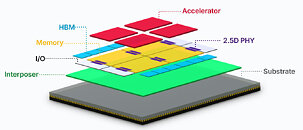
During MWC, Fujitsu partnered with networking equipment maker 1FINITY to unveil the first silicon wafers and an engineering sample of its "MONAKA" CPU. Scheduled for release in 2027, the initial Fujitsu MONAKA CPU utilizes the Armv9-A architecture and a 3D chiplet layout that combines a core die with separate SRAM and I/O dies. A single chip features 144 cores, and two-socket configurations can scale up to 288 cores per node. The platform supports 12-channel DDR5, PCIe 6.0 with CXL 3.0, and Arm SVE2 for AI and HPC workloads. Fujitsu has chosen TSMC to manufacture this chip using the 2 nm node, paired with Broadcom's 3.5D eXtreme Dimension System-in-Package (XDSiP) packaging architecture. This packaging allows MONAKA to become a 144-core design featuring four 36-core chiplets. These chiplets are stacked face-to-face with SRAM tiles through hybrid copper bonding, utilizing TSMC's N5 process for the cache layer.

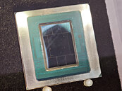
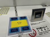
In the pictures below, we can see the silicon complex in its early sample packaging, which shows a large central I/O die, HBM memory around the CPU, and the new packaging technology. Reportedly, this CPU has already reached a working version, with Broadcom shipping the CPU to Fujitsu in late February this year. After initial testing and early performance validation, Fujitsu plans to ship these processors to customers around summer, with mass shipping to commence in 2027. The company envisions this SoC as a powerhouse for AI inference, simulation, and large-scale data processing. It will sell these systems to external customers, who showed great interest in Fujitsu's A64FX when the Fugaku computer came online. Fugaku was the most powerful supercomputer back in 2020, achieving 415.53 PetaFLOPS of FP64 and an impressive HPL-AI score of 1.421 ExaFLOPS using lower FP16 precision. Hence, we expect the new MONAKA CPU to enable much greater speeds and some efficiency improvements as well.

NVIDIA Offers "Vera" CPU as a Standalone Competitor to Intel's Xeon and AMD's EPYC Processors

NVIDIA's integration of AI systems now extends beyond GPUs with generic Arm CPUs. The company is introducing its high-performance "Vera" CPUs as a standalone product, marking its first entry as a competitor to Intel Xeon and AMD EPYC server-grade CPUs. NVIDIA CEO Jensen Huang confirmed this new venture in an interview with Bloomberg, stating, "For the very first time, we're going to be offering Vera CPUs. Vera is such an incredible CPU. We're going to offer Vera CPUs as a standalone part of the infrastructure. You can now run your computing stack not only on NVIDIA GPUs but also on NVIDIA CPUs. Vera is completely revolutionary... Coreweave will have to act quickly if they want to be the first to implement Vera CPUs. We haven't announced any of our CPU design wins yet, but there will be many."

The "Vera" CPU is equipped with 88 custom Armv9.2 "Olympus" cores that utilize Spatial Multithreading technology, allowing it to handle 176 threads through physical resource partitioning. These custom cores support native FP8 processing, enabling some AI workloads to be executed directly on the CPU with 6x128-bit SVE2 implementation. The chip offers 1.2 TB/s of memory bandwidth and supports up to 1.5 TB of LPDDR5X memory, making it ideal for memory-intensive computing tasks. However, with the CPU now being offered as a standalone solution, it is unclear whether there will be any classic memory options like DDR5 RDIMMs, or if the CPU will rely solely on SOCAMM LPDDR5X. A second-generation Scalable Coherency Fabric provides 3.4 TB/s of bisection bandwidth, connecting the cores across a unified monolithic die and eliminating the latency issues common in chiplet architectures. Additionally, NVIDIA has integrated a second-generation NVLink Chip-to-Chip technology, delivering up to 1.8 TB/s of coherent bandwidth for external "Rubin" GPUs.

Fujitsu Details Upcoming Arm-Based Monaka Processor Roadmap

Fujitsu has shared new details on its upcoming Arm-based Monaka processors during its Technology Update 2025 event. Monaka is planned as the company's next major datacenter CPU line, with the first chips arriving in 2027 on a 2 nm process. The initial Fujitsu Monaka CPU uses the Armv9-A architecture and a 3D chiplet layout combining a core die with separate SRAM and I/O dies. A single chip carries 144 cores, with two-socket configurations scaling to 288 cores per node. The platform supports 12-channel DDR5, PCIe 6.0 with CXL 3.0, and Arm SVE2 for AI and HPC workloads. Fujitsu is positioning it as a high-efficiency part aimed at AI inference, simulation, and large-scale data processing.

From there, the roadmap moves into more specialized designs. Targeted for late 2029, Monaka-X is a CPU-only built on a 1.4 nm class process. Fujitsu says it will be the first server CPU to implement Arm SME (Scalable Matrix Extension). The chip uses a 3D many-core layout tightly coupled with a GPU and includes hardware confidential-computing features as standard. The next CPU will be Monaka-X with NPU planned for the second half of 2030. This variant adds an on-package NPU aimed at mid-sized LLMs. Fujitsu is exploring a reconfigurable engine plus a dedicated quantization accelerator. Arriving in 2031, Monaka-XX is described as a full CPU-NPU fusion chip, again planned to be built on 1.4 nm or newer nodes. Overall, the roadmap shows Fujitsu pushing deeper into high-core-count Arm servers with increasing AI acceleration built directly into the platform.

Microsoft Readies Windows-on-Arm for Gaming With AVX/AVX2 Support

With the release of the October 2025 cumulative update (KB5066835) for Windows 11 versions 24H2 and 25H2, Microsoft has expanded Prism emulation for Arm64 devices. This update enables Windows to emulate x86 vector instructions such as AVX and AVX2 on Arm PCs. As a result, many apps and games that previously couldn't run on Arm hardware can now at least launch. Intel's AVX is a set of SIMD instructions commonly used by media tools, game engines, and creative applications to speed up tasks like video encoding, physics, and effects. Arm-based chips like Snapdragon do not natively support Intel's proprietary AVX instructions, which often led to failures or poor performance in these programs. Prism's emulation translates AVX instructions, allowing these programs to run on Arm devices. However, because it is emulation, there is additional CPU overhead, and performance will vary significantly depending on the application.

Arm, on the other hand, offers the Scalable Vector Extension (SVE), which enhances vector processing capabilities in the Armv8-A architecture, with SVE2 being its successor in Armv9-A. Unlike traditional SIMD designs with fixed-size vectors, SVE supports flexible vector lengths from 128 to 2048 bits in 128-bit increments. This flexibility allows chip manufacturers to select the vector size that best suits their processors. The main advantage is that programs written for SVE can run on any SVE-compatible processor without recompilation, regardless of the processor's vector size.
Return to Keyword Browsing
Nov 14th, 2026 02:02 CST change timezone

New Forum Posts

Popular Reviews

TPU on YouTube

Controversial News Posts