Monday, March 9th 2026

Fujitsu Showcases "MONAKA" CPU Sample with 3.5D XDSiP Packaging
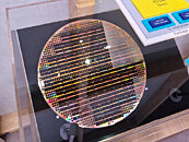
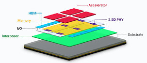
During MWC, Fujitsu partnered with networking equipment maker 1FINITY to unveil the first silicon wafers and an engineering sample of its "MONAKA" CPU. Scheduled for release in 2027, the initial Fujitsu MONAKA CPU utilizes the Armv9-A architecture and a 3D chiplet layout that combines a core die with separate SRAM and I/O dies. A single chip features 144 cores, and two-socket configurations can scale up to 288 cores per node. The platform supports 12-channel DDR5, PCIe 6.0 with CXL 3.0, and Arm SVE2 for AI and HPC workloads. Fujitsu has chosen TSMC to manufacture this chip using the 2 nm node, paired with Broadcom's 3.5D eXtreme Dimension System-in-Package (XDSiP) packaging architecture. This packaging allows MONAKA to become a 144-core design featuring four 36-core chiplets. These chiplets are stacked face-to-face with SRAM tiles through hybrid copper bonding, utilizing TSMC's N5 process for the cache layer.
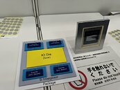
In the pictures below, we can see the silicon complex in its early sample packaging, which shows a large central I/O die, HBM memory around the CPU, and the new packaging technology. Reportedly, this CPU has already reached a working version, with Broadcom shipping the CPU to Fujitsu in late February this year. After initial testing and early performance validation, Fujitsu plans to ship these processors to customers around summer, with mass shipping to commence in 2027. The company envisions this SoC as a powerhouse for AI inference, simulation, and large-scale data processing. It will sell these systems to external customers, who showed great interest in Fujitsu's A64FX when the Fugaku computer came online. Fugaku was the most powerful supercomputer back in 2020, achieving 415.53 PetaFLOPS of FP64 and an impressive HPL-AI score of 1.421 ExaFLOPS using lower FP16 precision. Hence, we expect the new MONAKA CPU to enable much greater speeds and some efficiency improvements as well.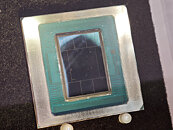
Source:
PC Watch Japan
In the pictures below, we can see the silicon complex in its early sample packaging, which shows a large central I/O die, HBM memory around the CPU, and the new packaging technology. Reportedly, this CPU has already reached a working version, with Broadcom shipping the CPU to Fujitsu in late February this year. After initial testing and early performance validation, Fujitsu plans to ship these processors to customers around summer, with mass shipping to commence in 2027. The company envisions this SoC as a powerhouse for AI inference, simulation, and large-scale data processing. It will sell these systems to external customers, who showed great interest in Fujitsu's A64FX when the Fugaku computer came online. Fugaku was the most powerful supercomputer back in 2020, achieving 415.53 PetaFLOPS of FP64 and an impressive HPL-AI score of 1.421 ExaFLOPS using lower FP16 precision. Hence, we expect the new MONAKA CPU to enable much greater speeds and some efficiency improvements as well.


4 Comments on Fujitsu Showcases "MONAKA" CPU Sample with 3.5D XDSiP Packaging
dragonball.fandom.com/wiki/Monaka
I wish I could spare 0.5 dimension just to play around
If it has an interposer and stacked active chips then it's 3D.
Too masive to be one-dimensional but with too many holes to be two-dimensional.
The same applies for thing between 2D and 3D.I would like to add half dimension to my flat to get more storage ...