News Posts matching #Sandy Bridge

Return to Keyword Browsing

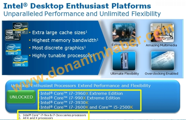
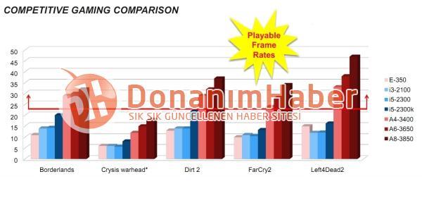
Intel Aims at 10 nm Processors by 2018

It's not just host nations of the Olympics that are decided almost decades in advance, but also Intel's silicon names and the fab process they're going to be built on. Intel has its plan for the greater part of this decade already charted out, well beyond the upcoming Ivy Bridge architecture. Intel follows the "tick-tock" product cycle, where every micro-architecture gets to be built on two succeeding fab processes, and every fab process getting to have two succeeding micro-architectures built on it, in succession. Westmere is an optical shrink of the Nehalem architecture, it was a "tick" for the 32 nm process, Sandy Bridge is its "tock", and a new architecture. Ivy Bridge is essentially an optical shrink of Sandy Bridge, it is the "tick" for 22 nm process.

Ivy Bridge will make its entry through the LGA1155 platform in 2012, it will make up the 2012 Core processor family. Haswell is the next-generation architecture that succeeds Sandy Bridge and IvyBridge, it will be built on the 22 nm process, and is expected to arrive in 2013. Roswell is its optical shrink to 14 nm, slated for 2014. Looking deep into the decade, there's Skylake architecture, that will span across 14 nm and 10 nm processes with Skymont. This model ensures that Intel has to upgrade its fabs every 2 or so years, an entirely new micro-architecture every 2 or so years as well, while providing optical shrinks every alternating year. Optical shrinks introduce new features, increased caches, and allow higher clock speeds. 10 nm for processors by 2018 sounds realistic looking at the advancement of NAND flash technologies that are pushing the boundaries of fab process development. NAND flash is much less complex than processor development, and hence serve as good precursors to a new process.

Core i7-3960X About 47% Faster On Average Than Core i7-990X: Intel

Slides of a key presentation to Intel's partners was leaked to sections of the media, which reveal Intel's own performance testing of the Core i7-3960X Extreme Edition, the top-model of the socket LGA2011 "Sandy Bridge-E" processor series. Meet the family here. In its comparison, Intel maintained the Core i7-990X Extreme Edition socket LGA1366 processor as this generation's top offering. It was pitted against the Core i7-3960X in a battery of tests that included some enthusiast favourites such as Cinebench 11.5, POV-Ray 3.7, 3DMark 11 physics, Pro-Show Gold 4.5, and some OEM favourites such as SPECint_rate base2006, SPECfp_rate base2006, and SiSoft SANDRA 2011B multimedia and memory bandwidth.

From these test results, the Core i7-3960X Extreme Edition is pitched to be about 47.25% faster on average, compared to Core i7-990X Extreme Edition. Intel is attributing the performance boost, apart from the normal IPC increase, to the 33% higher bandwidth thanks to the quad-channel DDR3 IMC, and the new AVX instruction set that accelerates math-heavy tasks such as encoding. The Core i7-3960X Extreme Edition is an upcoming socket LGA2011 six-core processor that is clocked at 3.30 GHz, with Turbo Boost speed of up to 3.90 GHz, with 12 threads enabled by HyperThreading technology, and 15 MB L3 cache. It will release by either late 2011 or early 2012.

Sandy Bridge-E Model Numbers, Clock Speeds Surface

Here are details of the first three models of Intel's "Sandy Bridge-E" Core i7 processors in the LGA2011 package. Some of these details were made public as early as mid-April. It was then analyzed that Intel was driving two distinct lines of LGA2011 client processors: Enthusiast and Performance, and within Performance, there were BClk multiplier-unlocked six-core, and locked quad-core chips. With the new series, Intel will move to the 3000 series of processor model numbering, indicating that the new processors will be part of Intel's 3rd generation Core processors, even though they're based on the Sandy Bridge architecture.

Before we move to the model numbers, here's a quick run up of the brand extenders. "X" denotes Extreme Edition, "K" denotes "Unlocked" (BClk multipler unlocked). Leading the pack will be Core i7-3960X Extreme Edition. This six-core (6 cores, 12 threads with HTT) chip has a nominal clock speed of 3.30 GHz, Turbo Boost speed of up to 3.90 GHz, and features the full 15 MB of L3 cache present on the Sandy Bridge-E silicon. Expect this chip to have a four figure price-tag.

Intel To Still Launch Sandy Bridge-E in 2011, But With Reduced Platform Feature-Set

Sandy Bridge-E is Intel's next-generation high-end desktop and enterprise platform that is an upscale of the Sandy Bridge platform the company launched early this year. At this year's major trade-shows such as Computex, motherboard partners displayed their socket LGA2011 motherboards with the complete feature-set of the platform. Apart from the large socket, and memory slots at odd places, the most distinct feature of those motherboards was the plethora of SATA ports they came with. Even the most [relatively] low-end LGA2011 motherboards had around 10 SATA ports, most of which were 6 Gb/s. Platform schematics also made it to the public domain around that time, revealing a key feature that makes driving 8 SATA 6 Gb/s ports possible: a supplementary PCI-Express 3.0 x4 link between the X79 PCH and the LGA2011 processor, that adds 16 GB/s (8 GB/s per direction) of bandwidth between the processor and the chipset, without which the storage controller would be severely bottlenecked with the DMI Gen2 (physical PCI-Express 2.0 x4), with its puny 8 GB/s (4 GB/s per direction) bandwidth.

Originally slated for Q4 2011, Intel's Sandy Bridge-E platform was reported to have been delayed to Q1 2012. It is now emerging that Patsburg-D, the variant of Patsburg X79 chipset, which features 8 SATA/SAS 6 Gb/s ports, which requires that supplementary PCI-E 3.0 x4 link, may be causing a development hold up at Intel. So, the company is planning on launching the platform this year itself, but with Patsburg-B, a variant of the chipset that has only four SATA/SAS 6 Gb/s ports, and relies entirely on DMI as the chipset interconnect. The slide below lists out differences between the many variants of Patsburg PCH. DMI would give the platform the same amount of chipset interconnect bandwidth as today's LGA1155-Cougar Point platform. It is, however possible that the higher Patsburg-D/X variants will be launched when Intel irons out whatever issues exist with them.

ZOTAC Readies Monster LGA1155 Motherboard

ZOTAC entered the motherboard scene as yet another vendor of reference NVIDIA nForce motherboards, which the like of EVGA, XFX, and BFG also sold. After the fall of nForce, ZOTAC attempted a LGA1366 motherboard, and went dormant with motherboards. Later, it picked up interest in the mini-ITX form-factor as it gained popularity in Asian markets like China and India, manufacturing motherboards based on Intel Atom, Atom with NVIDIA ION, and eventually socketed mini-ITX motherboards as it became a 2-chip affair with Intel's Ibex Peak platform (LGA1156). It looks like Zotac is making a comeback into full-size ATX motherboards that target the very top tier of the market, to woo gamers, professional overclockers, and enthusiasts.

Seen here is what the Chinese press is referring to as "ZT-Z68 Crown Edition-U1DU3", we may have lost the correct name in translation, but let's call it ZT-Z68-U1DU3 for now. It is a full-size ATX motherboard that takes socket LGA1155 Intel Sandy Bridge and future Ivy Bridge processors, and is based on the Intel Z68 Express chipset. It combines a strong VRM to support extreme overclocking, with graphics expansion, adding 4-way NVIDIA SLI and AMD CrossFireX capabilities using an NVIDIA BR-03 bridge-chip that sits on the processor's PCI-E x16 link, to give out two PCI-Express 2.0 x16 links, which are then spread between four slots in x16/NC/x16/NC, x16/NC/x8/x8, or x8/x8/x8/x8 lane configurations.

AMD FX-8130P Processor Benchmarks Surface

Here is a tasty scoop of benchmark results purported to be those of the AMD FX-8130P, the next high-end processor from the green team. The FX-8130P was paired with Gigabyte 990FXA-UD5 motherboard and 4 GB of dual-channel Kingston HyperX DDR3-2000 MHz memory running at DDR3-1866 MHz. A GeForce GTX 580 handled the graphics department. The chip was clocked at 3.20 GHz (16 x 200 MHz). Testing began with benchmarks that aren't very multi-core intensive, such as Super Pi 1M, where the chip clocked in at 19.5 seconds; AIDA64 Cache and Memory benchmark, where L1 cache seems to be extremely fast, while L2, L3, and memory performance is a slight improvement over the last generation of Phenom II processors.

Intel Ivy Bridge Dual-Core Put Through Clock-to-Clock Benches Against Sandy Bridge

Taiwanese PC enthusiast Coolaler has a new Ivy Bridge LGA1155 dual-core engineering sample to play with, and wasted no time in putting it through some tests. The sample has two cores, four threads with HyperThreading enabled, clock speed of 1.80 GHz, 256 KB L2 cache per core, and 4 MB shared L3 cache. It is running on an Intel P67 chipset-based motherboard with 8 GB of dual-channel DDR3-1600 MHz memory. At 1.80 GHz, it may not be game for absolute performance figures since it's unlikely that Intel will release a chip with that clock speed unless it has unreal performance:clockspeed gains over Sandy Bridge; but it's good enough for clock-to-clock performance comparisons between Ivy Bridge and Sandy Bridge. A Core i5-2400 was clocked at 1.80 GHz with 18x BClk multiplier, and put through a single-threaded benchmark, and a multithreaded one.

The cache and memory benchmark that measures bandwidth and latency of caches and memory was unable to measure bandwidth, but measured some latencies. The L1 cache at 2.2 nanoseconds (ns), and L2 at 2.9 ns. Next, the Ivy Bridge DC, and the Core i5-2400 (@ 1.80 GHz) testbeds were put through CPUMark 99, where Ivy Bridge DC scored 278 points, and Core i5-2400 clocked at 1.80 GHz scored closely followed at 276 points. Moving on to multithreaded performance, the two were put through Cinebench 11.5 64-bit. The Ivy Bridge DC chip scored 1.81 points; while the Core i5-2400 clocked at 1.80 GHz, scored 2.61 points. Coolaler promises more benches.

Sandy Bridge-E Delayed to January 2012: Sources

Originally slated for Q4 2011, the launch of Intel's Sandy Bridge-E desktop/workstation platform has been pushed back to Q1 2012, sources told VR-Zone. The high-end platform was expected by industry observers to be a December launch, targeting the shopping season, but it seems like January 2012 is found to be more fitting. Perhaps the International CES, where the latest and greatest from the tech industry is unveiled, serves as the ideal launch-pad for Sandy Bridge-E.

Sandy Bridge-E is an upscale of the architecture that makes up Intel's 2011 Core processor family. Consisting of 4 or 6 cores, Sandy Bridge makes up two distinct product lines for the client desktop market. The chips pack massive quad-channel DDR3 integrated memory controllers and PCI-Express 3.0 hubs that can drive up to four graphics cards. The processor is made of a new 2011-pin LGA package, with the new Intel X79 chipset handling the rest of the platform.

AMD Introduces Vision A6-3650 and A8-3850 Desktop APUs

AMD announced two of its first Vision A-Series accelerated processing units (APUs) for desktops today. Built in the socket FM1 package, the A6-3650 and A8-3850 are fabricated on the 32 nm HKMG process. Both pack four x86-64 cores, and while the A6 has 320 stream processors in the GPU component, the A8 has 400 of them. Both chips have 4 MB of cache, dual-channel DDR3-1866 MHz IMCs, and PCI-Express 2.0 hubs to drive discrete graphics.

The AMD A8-3850 has its four x86-64 cores clocked at 2.90 GHz, with the Radeon HD 6550D GPU engine clocked at 600 MHz. This chip has a TDP of 100W, it is priced at US $135. The AMD A6-3650 has its CPU component clocked at 2.60 GHz, and Radeon HD 6530D GPU engine clocked at 443 MHz. This chip goes for US $115. With these two, AMD is targeting higher models of Sandy Bridge-based Pentium Dual-Core and Core i3 Sandy Bridge chips. Both will be available in stores by July 3.

ASRock Readies Z68 Fatal1ty Motherboard with PCI-Express 3.0 Slots

ASRock gave its premium LGA1155 motherboard lineup a boost with the new Z68 Fatal1ty. Apart from being a Z68 chipset based motherboard modeled along the lines of its predecessor, the ASRock P67 Fatal1ty, the new motherboard features PCI-Express 3.0 graphics slots, that work on Sandy Bridge and future Ivy Bridge processors. The new third generation PCI-E interconnect can drive 1 GB/s of data per link, per direction. You'll need PCI-E 3.0 compliant add-on cards to make use of that bandwidth, current graphics cards will run at Gen. 2 speeds. One advantage here could be that AMD Radeon HD 5000 and HD 6000 series single-GPU graphics cards will run on Gen 2.1 mode, which has slightly higher bandwidth at its disposal thanks to its lower-overhead data coding scheme.

The ASRock Z68 Fatal1ty is designed for both gamers and overclockers, using high-grade components. The LGA1155 socket is powered by a 18-phase VRM, wired to four DDR3 DIMM slots supporting dual-channel DDR3-2133 MHz (Ivy Bridge IMC's optimal memory speed). Featuring Intel Flexible Display Interface (FDI), the board allows you to use the integrated graphics. With the Lucid Virtu technology, you can switch between the integrated graphics, and discrete graphics cards. Expansion slots include two PCI-Express 3.0 x16 (electrical x8/x8 when both are populated), one PCI-Express 2.0 x16 (electrical x4, wired to Z68 PCH), and two each of PCI-E 2.0 x1 and legacy PCI.

Apacer Announces ARES DDR3-2133 MHz Dual Channel Memory Kits for Overclocking

Apacer, one of the world's leading brands of memory modules, today announced an expansion of its ARES overclocking memory series with high capacity and clock rate: DDR3-2133 8GB (4GBx2) dual channel memory kit,which is engineered for the latest Intel P67 and Z68 Sandy Bridge platforms. With a combination of high clock rate, huge capacity and low latency of CL9, ARES series is a perfect solution for extreme PC enthusiasts and gamers who want to optimize performance on the new platforms.

The newly-unveiled ARES DDR3-2133 8GB dual channel memory kit provides the highspeed and capacityon the Intel P67 and Z68 Sandy Bridge platforms and is backwards compatible with existing the P55 platform. It runs at CL9-11-9-27 with 1.65 voltage, using advancedprocess 256Mb x 8chips, which are screened and tested withthe advanced test fixture and programs under diversified parameters of voltage and time sequences.

EVGA Readies Dual-LGA2011 X79 Motherboard

At this year's Computex event, we were treated to socket LGA2011 motherboards by various motherboard manufacturers, except EVGA. The company makes some of the highest grade enthusiast motherboards in the Intel platform, and so it was missed. It is however, said to be working on a monstrous dual-socket LGA2011 motherboard based on the Intel X79 chipset, that would replace its dual-socket LGA1366 EVGA SR-2.

Just imagine, such a monstrosity would combine two six/eight/twelve-core LGA2011 Sandy Bridge-E processors with eight channels of DDR3 memory, and four PCI-Express 3.0 x16 (electrical x16) links to drive its graphics cards and connectivity. EVGA said that it will have single-socket LGA2011 motherboards by the time the platform launches, and this dual-LGA2011 about a month later.

MSI Offers Premium Embedded Solution IM-QM67 with Intel Sandy Bridge Processor

MSI, the global leading brand in motherboards, announced the upgraded version of IM-QM67 which is powered by the 2nd generation Intel Core processor family, Intel Sandy Bridge processor, and Intel QM67 Express chipset. IM-QM67 supports multiple display outputs in a mini-ITX form factor board and utilizes Intel's 32nm process technology products to give the competitive advantage through the performance enhancements and scalability.

MSI debuts the IM-QM67 based on the Intel Core i7, Core i5 and Core i3 processors to offer lower power consumption and enhanced graphic and media performance. The IM-QM67 is equipped with dual-channel DDR3 1067/1333/1600 MHz memory up to a maximum of 16 GB in dual SO-DIMM slots and is ideally suited to applications requiring multi-tasking capabilities, high computing power. This combination of CPU, chipset and memory provides the MSI IM-QM67 with improved power efficiency and high-speed data transfer for performance-driven industrial applications, such as industrial control, automation, digital signage, kiosk, POS, gaming, ATM and medical electronic.

ZOTAC Z68-ITX WiFi a Fun-Sized Treat for Overclockers

Rarely do motherboard vendors dish out mini-ITX form-factor motherboards targeting the overclocking community. There's little space to squeeze in the bare essentials, but nothing is impossible, if there are competent designers at work, a case in point is the new Z68-ITX WiFi from ZOTAC. Based on the Intel Z68 Express chipset, this board supports LGA1155 Core i3/i5/i7 Sandy Bridge, and future Ivy Bridge processors, supports their integrated GPU giving you access to Intel QuickSync technology, as well as a suite of overclocking options.

To begin with the LGA1155 socket is powered by an 8-phase digital-PWM power design that uses high-grade PWM chokes made by Pulse, and in all probability, a Volterra PWM IC giving you precise voltage control as well as vDroop protection (high-precision load-line calibration). It also uses server-grade high-C capacitors. The PWM circuit takes input from an 8-pin EPS connector. The PWM chips are cooled by a large heatsink that sends some of its heat to the heatsink cooling the Z68 PCH, over a heat pipe.

MSI New Z68A-GD80 Swims in PCI-Express 3.0 Fame

While Sandy Bridge-E LGA2011 processors will come with integrated PCI-Express 3.0 hubs, they're still a couple of quarter financial years away. Meanwhile, MSI jumped the gun on its latest socket LGA1155 Intel Z68-based motherboard with not only support for Intel's upcoming 22 nm Ivy Bridge LGA1155 processors, but also the PCI-Express 3.0 hubs that the new processors come with. While Ivy Bridge has PCI-E 3.0 hub, not just any LGA1155 motherboard can give you PCI-E 3.0 support. It requires slots that are compliant with the new specification, and needs PCI-E 3.0 compliant external switching chips. MSI has both, on its new Z68A-GD80 motherboard, and with it, the bragging rights of being the world's first PCI-E 3.0 compliant motherboard.

PCI-Express 3.0 gives you twice the interface bandwidth as PCI-Express 2.0, which means that PCI-Express 3.0 x8 has the same bandwidth as PCI-Express 2.0 x16. But before you celebrate, let's remind ourselves that you also need a PCI-E 3.0 compliant GPU to make the slots operate at Gen 3.0 speeds. Installing PCI-Express 2.0 GPUs on Gen 3.0 won't run the slots at Gen 3.0 speeds. That aside, the Z68A-GD80 is a sufficiently-equipped enthusiast motherboard featuring 14-phase VRM for the CPU, dual-channel DDR3-2133 support, two PCI-E 3.0 x16 slots (x8/x8 with populated), a third PCI-E x16 wired to the Z68 PCH, running at PCI-E 2.0 x4 speeds, and a couple of PCI-E 2.0 x1 and legacy PCI. There are three internal SATA 6 Gb/s ports; eSATA, USB 3.0, make for the rest of the connectivity. There is full-fledged display connectivity, with Lucid Virtu support. Expect this board to be out any time soon.

ASRock X79 Extreme4 Pictured

ASRock is ready with what it will be offering the very top tier of consumers of the Sandy Bridge-E platform, the third largest selling motherboard vendor is ready with the X79 Extreme4. This standard-size ATX motherboard uses essentially the same component layout as most socket LGA2011 boards we've seen so far. The LGA2011 socket is powered by an 8-phase VRM. The socket is wired to four DDR3 DIMM slots on its either sides, to support quad-channel DDR3-2133 MHz memory. The processor also holds a massive 40-lane PCI-Express 3.0 hub, giving out two PCI-Express 3.0 x16 links, distributed between three slots (as x16/x16/NC or x16/x8/x8), with two each of PCI-E x1 and PCI in between.

ASRock did not finalize its chipset/VRM heatsinks design, yet. While we can't see the right portion of the board in the picture, we can assume that all 10 SATA 6 Gb/s and 2 SATA 3 Gb/s ports will be internal ports, with the possibility of one or two eSATA. Other connectivity includes 8-channel HD audio, dual gigabit Ethernet, and four USB 3.0 ports (two by header). The board supports 3-way NVIDIA SLI and AMD CrossFireX.

Gigabyte X79 UD3 LGA2011 Motherboard First Shot

Here is the first picture of GA-X79A-UD3, the first Gigabyte-branded socket LGA2011 motherboard. Based on the Intel X79 Express chipset, the board supports upcoming Sandy Bridge-E enthusiast processors in the LGA2011 package. Mind you, this is just the cheapest LGA2011 board from Gigabyte, there is a higher-end line of X79 motherboards, so don't let the unspectacular looks of the UD3 get you.

The GA-X79A-UD3 is a standard ATX sized motherboard. Its main VRM is spread all around the large CPU socket, in what appears to be a 6-phase design, with an unknown number of memory and uncore phases. LGA2011 processors feature a large quad-channel DDR3 memory controller, along with a northbridge uncore component with a 40-lane PCI-Express 3.0 controller. Those amount to the socket's insane pin-count of 2,011 pins. Memory slots are located in pairs of two on either sides of the socket. Each slot is its own 64-bit wide memory channel.

ASUS Readies Z68-based ROG Maximus IV Extreme-Z Motherboard

When Intel's Sandy Bridge platform was launched, P67 Express was perceived as the top of the line discrete graphics chipset that gives performance segment users everything they'll ever need. ASUS hence based its prestigious ROG Maximus branded motherboard based on it, and came up with the Maximus IV series. With Intel releasing a higher-end chipset with the Z68 Express, ASUS decided to redo its socket LGA1155 ROG motherboard lineup, with the Maximus IV Extreme-Z. The new motherboard gives users access to the processors' embedded graphics via a HDMI port, and gives them the benefit of Intel Smart Response technology that P67 lacks.

The Maximus IV Extreme-Z looks similar to its P67-based cousin. Based on the Intel Z68 chipset, the motherboard uses an NVIDIA nForce 200 bridge chip to ensure PCI-Express connectivity to up to four graphics cards, supporting NVIDIA SLI and AMD CrossFireX. The CPU is powered by ASUS Digi+ Extreme VRM, backed by high-grade components and proadlizers to condition power. There are four DIMM slots supporting dual-channel DDR3-2000 MHz memory by overclocking. Expansion slots include four PCI-Express 2.0 x16 (x16/NC/x16/NC or x8/x8/x8/x8), there's also a PCI-E x1 and open-ended PCI-E x4.

Eurocom Launches Line of the Most Powerful Optimus Notebooks

The Eurocom Optimus line are performance-oriented business and gaming-friendly notebooks based on Intel's Sandy Bridge technology with discrete NVIDIA GT 555M graphics and longer battery life thanks to NVIDIA Optimus Technology. NVIDIA Optimus technology intelligently optimizes your notebook PC, providing the outstanding graphics performance you need, when you need it, all the while extending battery life for longer enjoyment. They are built around the Intel Huron River HM65 platform and support Intel's mobile line of Sandy Bridge Core i7, i5 and i3 processors.

New Sandy Bridge Based Celeron Processors Detailed

Amidst the rather high-profile launch of Intel's Z68 chipset platform, Intel Smart Response technology, and Larson Creek SSDs, Intel is also readying its cheapest processors for the LGA1155 platform, this time carrying the Celeron brand. Based on the new Sandy Bridge processor architecture, the single-core Celeron G440, and dual-core Celeron G530, Celeron G540 processors stick to the very basics in terms of feature set.

The chips lack Intel HyperThreading or CPU Turbo Boost, run at low clock speeds, and have just 2 MB of L3 cache enabled. The G440 is a single-core/single-thread chip clocked at 1.60 GHz, with 650 MHz graphics (1.00 GHz Turbo), and 35W TDP. The G530 puts on a second core, is clocked at 2.40 GHz, with 850 MHz (1.00 GHz Turbo) graphics, and 65W TDP. The series is topped off with G540 dual-core, which is clocked at 2.5 GHz. Expect these chips to take up sub-$100 price points.

BIOSTAR Announces New T-Series TZ68A+ Motherboard

BIOSTAR MICROTECH INT'L CORP., A professional manufacturer of motherboards, introduces Intel Z68 chipset based motherboard that supports Intel 2nd generation Sandy Bridge processor family, it is special designed for advanced gamers and overclocking fans. BIOSTAR "TZ68A+", the only solution supports both built-in graphics and external overclocking among Intel Sandy Bridge processors; it is also equipped with Lucid Virtu GPU Virtualization - a dynamic switching between built-in processor graphics and high-end 3D performance discrete graphics cards. Moreover, it also fully supports Intel Smart Response Technology - enabling SSD like performance with HDD capacity.

AMD A-Series APUs Tested Against Sandy Bridge CPUs at Gaming on IGP

What happens when you pit Intel's "Visually Smart" Sandy Bridge processors against Radeon-enriched AMD Fusion A-Series accelerated processing units? They do terribly at gaming on integrated graphics. Surprise! That is notwithstanding the fact that AMD is pitching its A-Series Fusion APUs to be a lot more than CPUs with embedded GPUs, they're pitched to be processors that make lower-mainstream graphics pointless, and to alter the software ecosystem to be more GPGPU intensive, so applications could benefit from the over 500 GFLOPs of computation power the 400 stream processor DirectX 11 GPU brings to the table.

A leaked presentation slide shows AMD's performance projections for the A-Series GPU, tests included GPU-heavy DirectX 10 titles such as Crysis Warhead and Borderlands; as well as DirectX 11 ready titles such as Dirt 2. AMD's quad-core A8-3850, A8-3650 and A8-3450 were included alongside Intel's dual-core Sandy Bridge Core i3-2100, and quad-core Core i5-2300, Core i5-2500K. The Atom-competitive E350 Zacate dual-core was also in the comparision, perhaps to show that it is nearly as good as Intel's much higher segment Core series processors at graphics.

ASUS Announces P8Z68 Series and Maximus IV Gene-Z LGA1155 Motherboards

Continuing its legacy of leadership, ASUS offers consumers a range of new motherboards based on the Intel Z68 Express chipset. The ASUS P8Z68 Series and ROG Maximus IV GENE-Z motherboards all have numerous powerful features that fully exploit the performance benefits of Sandy Bridge technology without compromise, packing more features and new innovations onto the Z68 platform while maintaining unmitigated performance and reliability.

ASUS is the only motherboard manufacturer able to integrate diverse new technologies in tandem on its Z68-based motherboards on launch. These include the universal implementation of LucidLogix Virtu switchable graphics to harness the capabilities of Intel Quick Sync Video for faster video transcoding and the extreme performance of the latest NVIDIA and AMD graphics cards, along with Intel Smart Response Technology to accelerate hard drive performance and reduce energy consumption.

Gigabyte GA-Z68-UD3H-B3 Motherboard Pictured

It is becoming increasingly clear now, that Gigabyte will have two parallel lines of socket LGA1155 motherboards based on the same Intel Z68 B3 chipset, one that does away with display connectivity to make room for other ports and is geared for discrete graphics, while the other has display connectivity at the expense of additional ports on the rear panel, and also gives you everything you'd expect from Z68, including overclocking. In mid-April, pictures of GA-Z68-UD3P-B3 surfaced, which is a motherboard of the first kind explained above. Now, there's deck of pictures of the GA-Z68-UD3H-B3, its counterpart of the second kind.

The GA-Z68-UD3H-B3 features a much lighter CPU VRM, consisting of 7 phases, against 14 on the UD3P. It gives you the same expansion slot layout consisting of two PCI-Express 2.0 x16 (x8/x8 when both are populated), supporting ATI CrossFire and NVIDIA SLI, three PCI-E x1, and two PCI. Gigabyte made full use of the display connectivity options that come with Sandy Bridge, there is one each of DVI, D-Sub, HDMI, and DisplayPort. Audio is at the helm of Realtek ALC889 8+2 channel HD audio CODEC, with optical SPDIF output.

GIGABYTE Enters Long Term Partnership with LUCIDLOGIX

GIGABYTE TECHNOLOGY Co., Ltd, a leading manufacturer of motherboards, graphics cards and other computing hardware solutions today announced a new partnership with Lucidlogix, the makers of Virtu GPU virtualization technology. The partnership ushers in broad adoption of Virtu on future GIGABYTE 6 series motherboards, and sets the stage for long term cooperation between the two companies.

"We are excited about our new partnership with Lucid because of the huge potential for switchable graphics in the PC DIY market where GIGABYTE motherboards enjoy considerable market share," said Henry Kao, VP of R&D, at GIGABYTE. "We believe that Virtu will add considerable value to GIGABYTE motherboards using Intel's Sandy Bridge graphics and will provide our customers with the flexibility and choice they want from their system."
Return to Keyword Browsing
Apr 26th, 2024 13:52 EDT change timezone

New Forum Posts

Popular Reviews

Controversial News Posts