News Posts matching #Siemens

Return to Keyword Browsing

IBM and Siemens Collaborate on Research to Advance Nanostack Architecture

Today, IBM (NYSE: IBM), in collaboration with Siemens, announced new research aimed at advancing IBM's nanostack architecture, a new transistor architecture unveiled by IBM earlier this year. The collaboration will bring together IBM's leadership in semiconductor device innovation and Siemens' expertise in electronic design automation (EDA), process simulation, lithography optimization, and advanced manufacturing software to accelerate the development of nanostack.

Nanostack is the industry's first known three-dimensional, nanosheet-based design, vertically stacking and staggering transistors to pack more transistors onto a chip, with nearly 100 billion transistors in a space the size of a fingernail at its current 7 angstrom node. The design also unlocks the use of different material combinations within each stacked layer to optimize performance and power efficiency of each transistor independent of the other. These innovations power substantial leaps in energy efficiency, performance, and SRAM scaling.
Siemens Advances Self-verifying Agentic AI Workflows for Semiconductor and PCB Design

Siemens today announced an expansion of its strategic partnership with NVIDIA to deliver self-verifying agentic AI workflows to EDA, helping semiconductor and printed circuit board (PCB) engineering teams move from autonomous task orchestration toward more trusted, continuously validated engineering outcomes. The new capabilities build on Siemens' recently introduced Fuse EDA AI Agent system and add new NVIDIA AI technology to help long-running, domain scoped, AI agents reason, act and continuously validate decisions against deterministic, physics-based EDA engines.

The updates to Siemens' Fuse EDA AI Agent are designed to help the semiconductor and PCB industry move beyond simple automation and deliver trusted and verifiable outcomes that improve result quality, time-to-results, tool-calling reliability and token efficiency across long-running engineering workloads. The Fuse EDA AI Agent system is now integrated into Siemens' recently launched Intelligence Center X, supporting agent creation and orchestration in Siemens' enterprise industrial AI environment. Intelligence Center X delivers AI-driven, coordinated processes across design, manufacturing and supply chain - enhancing the comprehensive Digital Twin to support smarter execution and more trusted outcomes.

SPEC Updates SPECviewperf 15 Benchmark

The Standard Performance Evaluation Corporation (SPEC), the trusted global leader in computing benchmarks, today announced the availability of the SPECviewperf 15.0.1 benchmark, an important update to the worldwide standard for measuring graphics performance based on professional applications. This release introduces snx-05, a workload based on Siemens NX 2406, rounding out the benchmark's support for high-end computer-aided design (CAD) applications.

The new snx-05 workload represents the first "snap-in" workload enabled by SPECviewperf 15's modern architecture, which allows for the addition of new workloads without requiring users to re-run existing benchmarks. This workload utilizes the OpenGL graphics API and stresses standard OpenGL features, including vertex and pixel shaders, textures, and multisampled antialiasing.

Siemens and nVent to Release Joint Reference Architecture for NVIDIA AI Data Centers

As AI workloads grow more intensive and distributed, data center infrastructure strategies must balance performance, efficiency, and scalability through increasingly intelligent and adaptive systems. To support this next generation of digital infrastructure, Siemens and nVent are combining their expertise to help data centers prepare cooling and power infrastructure for global deployment and operational resilience.

The new joint architecture developed by Siemens and nVent has been created to help customers build 100 MW hyperscale AI data centers designed to house large-scale, liquid-cooled AI infrastructure like NVIDIA DGX SuperPOD with DGX GB200 systems. It presents a Tier III-capable architecture that integrates Siemens' industrial-grade electrical and automation systems with NVIDIA DGX SuperPOD reference designs and nVent liquid cooling technology.

"We have decades of expertise supporting customers' next-generation computing infrastructure needs," said Sara Zawoyski, president of nVent Systems Protection. "This collaboration with Siemens underscores that commitment. The joint reference architecture will help data center managers deploy our cutting-edge cooling infrastructure to support the AI buildout."

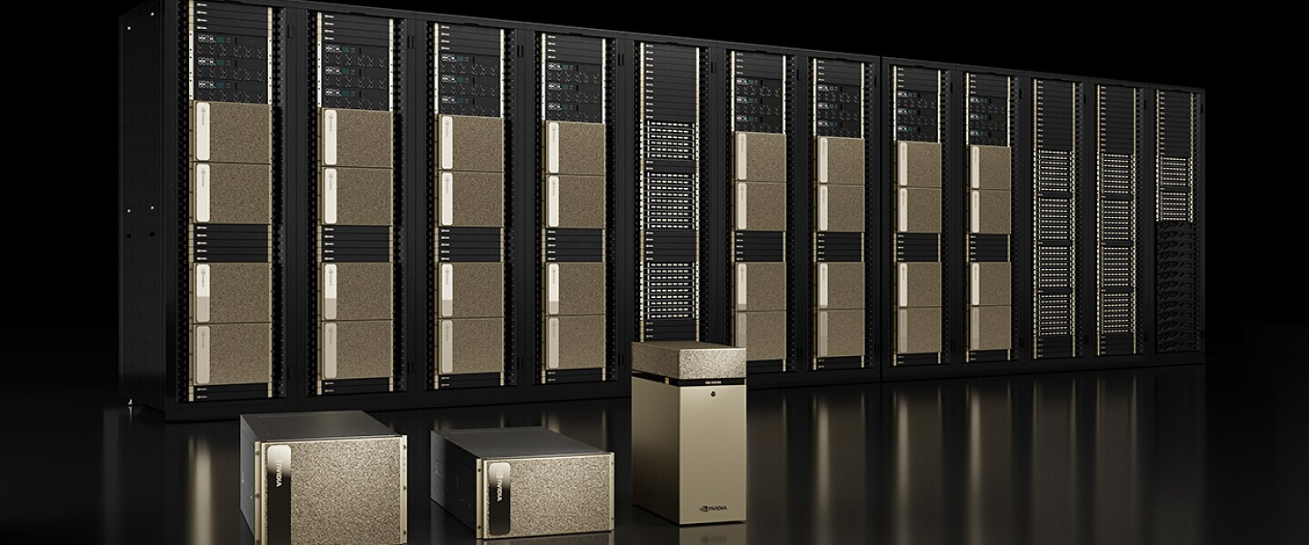
NVIDIA to Build Seven New AI Supercomputers for U.S. Government

NVIDIA today announced that it is working with the U.S. Department of Energy's national labs and the nation's leading companies to build America's AI infrastructure to support scientific discovery, economic growth and power the next industrial revolution.

"We are at the dawn of the AI industrial revolution that will define the future of every industry and nation," said Jensen Huang, founder and CEO of NVIDIA. "It is imperative that America lead the race to the future—this is our generation's Apollo moment. The next wave of inventions, discoveries and progress will be determined by our nation's ability to scale AI infrastructure. Together with our partners, we are building the most advanced AI infrastructure ever created, ensuring that America has the foundation for a prosperous future, and that the world's AI runs on American innovation, openness and collaboration, for the benefit of all."

Rapidus Announces Collaboration with Siemens for 2 nm Semiconductor Design

Rapidus Corporation, a manufacturer of advanced logic semiconductors, today announced a strategic collaboration with Siemens Digital Industries Software for semiconductor design and manufacturing processes for the 2 nm generation. Rapidus will collaborate with Siemens to jointly develop a process design kit based on the Calibre platform, the industry-standard verification solution that enables highly accurate and efficient physical verification, manufacturing optimization and reliability assessment from semiconductor design through to fabrication, while continuing to further its design and verification ecosystem.

This collaboration supports the manufacturing for design (MFD) concept advocated by Rapidus to achieve high yield and short turnaround time from the early stages of manufacturing. Further, Rapidus and Siemens EDA will build a reference flow that holistically supports design, verification and manufacturing from front-end to back-end. This reference flow provides a smooth development environment for Rapidus' Rapid and Unified Manufacturing Service (RUMS).

Intel Foundry Announces Reference Workflows from Ansys, Cadence, Siemens, and Synopsys

Today marks a new milestone in the growth of Intel Foundry's design ecosystem as key partners Ansys, Cadence, Siemens, and Synopsys have announced the availability of reference flows for Intel's embedded multi-die interconnect bridge (EMIB) advanced packaging technology. This comes on the heels of recent announcements where those same partners declared readiness for Intel 18A designs. "Today's news shows how Intel Foundry continues to combine the best of Intel with the best of our ecosystem to help our customers realize their AI systems ambitions," said Suk Lee, vice president for Ecosystem Development, Intel Foundry.

The success of Intel Foundry is rooted in collaboration with a vibrant design ecosystem. This ensures customers can access our leading process and packaging technologies. Now, in collaboration with our ecosystem partners, we are making it as easy and as fast as possible for companies to optimize, fabricate and assemble their system-on-chip designs through our foundries, while enabling their designers with validated EDA tools, design flows and IP portfolios for silicon-through-package design. This systems foundry approach allows our customers to innovate at every layer of the stack so they can meet the complex computing demands of the AI era, where chip architectures increasingly rely on multiple CPUs, GPUs and NPUs in a package to achieve performance requirements.

NVIDIA Modulus & Omniverse Drive Physics-informed Models and Simulations

A manufacturing plant near Hsinchu, Taiwan's Silicon Valley, is among facilities worldwide boosting energy efficiency with AI-enabled digital twins. A virtual model can help streamline operations, maximizing throughput for its physical counterpart, say engineers at Wistron, a global designer and manufacturer of computers and electronics systems. In the first of several use cases, the company built a digital copy of a room where NVIDIA DGX systems undergo thermal stress tests (pictured above). Early results were impressive.

Making Smart Simulations
Using NVIDIA Modulus, a framework for building AI models that understand the laws of physics, Wistron created digital twins that let them accurately predict the airflow and temperature in test facilities that must remain between 27 and 32 degrees C. A simulation that would've taken nearly 15 hours with traditional methods on a CPU took just 3.3 seconds on an NVIDIA GPU running inference with an AI model developed using Modulus, a whopping 15,000x speedup. The results were fed into tools and applications built by Wistron developers with NVIDIA Omniverse, a platform for creating 3D workflows and applications based on OpenUSD.

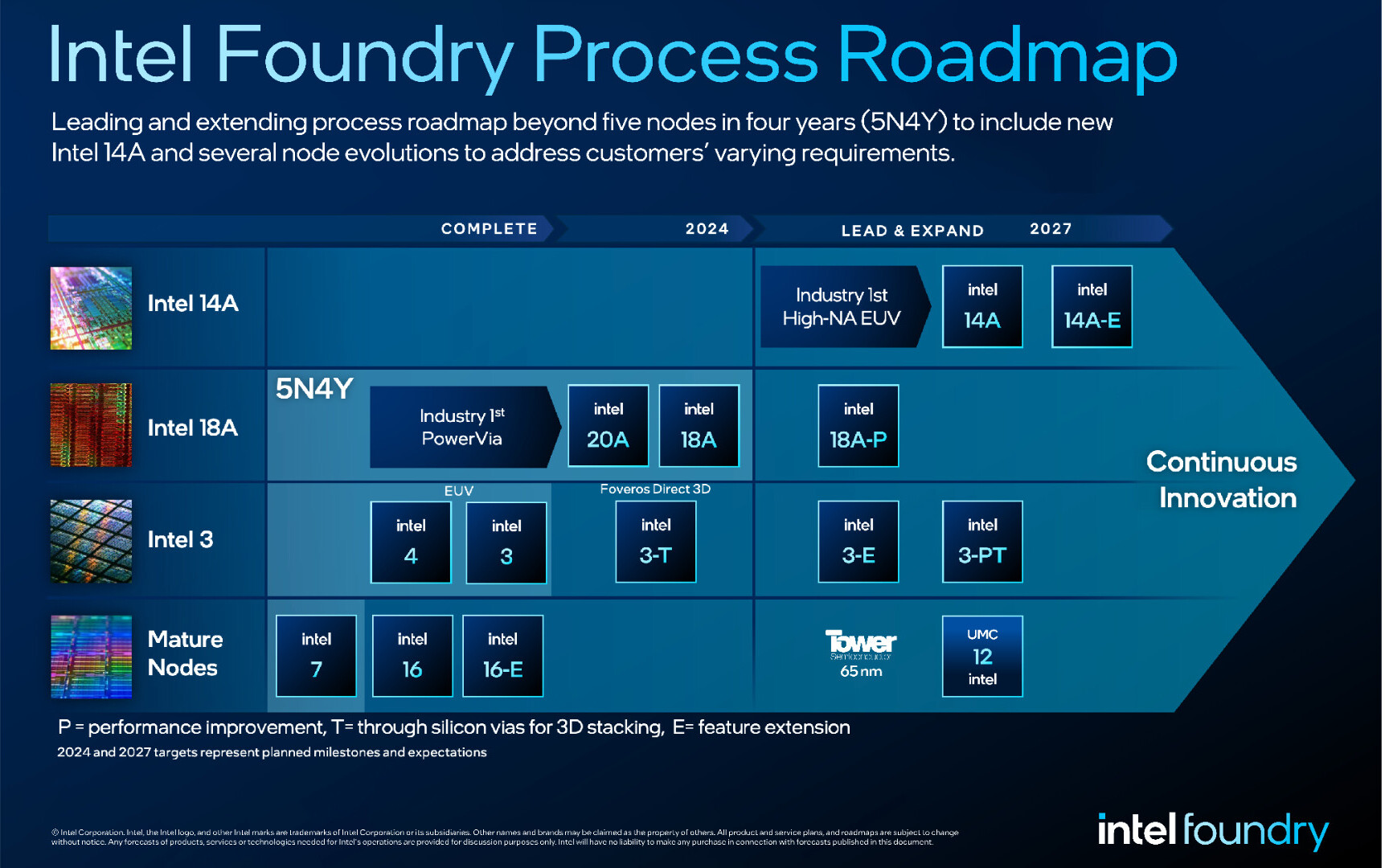
Intel Announces Intel 14A (1.4 nm) and Intel 3T Foundry Nodes, Launches World's First Systems Foundry Designed for the AI Era

Intel Corp. today launched Intel Foundry as a more sustainable systems foundry business designed for the AI era and announced an expanded process roadmap designed to establish leadership into the latter part of this decade. The company also highlighted customer momentum and support from ecosystem partners - including Synopsys, Cadence, Siemens and Ansys - who outlined their readiness to accelerate Intel Foundry customers' chip designs with tools, design flows and IP portfolios validated for Intel's advanced packaging and Intel 18A process technologies.

The announcements were made at Intel's first foundry event, Intel Foundry Direct Connect, where the company gathered customers, ecosystem companies and leaders from across the industry. Among the participants and speakers were U.S. Secretary of Commerce Gina Raimondo, Arm CEO Rene Haas, Microsoft CEO Satya Nadella, OpenAI CEO Sam Altman and others.

Siemens and Intel to Collaborate on Advanced Semiconductor Manufacturing

Siemens AG, a leading technology company, and Intel Corporation, one of the world's largest semiconductor companies, have signed a memorandum of understanding (MoU) to collaborate on driving digitalization and sustainability of microelectronics manufacturing. The companies will focus on advancing future manufacturing efforts, evolving factory operations and cybersecurity, and supporting a resilient global industry ecosystem.

"Semiconductors are the lifeblood of our modern economies. Few things run without chips. Therefore, we're proud to collaborate with Intel to quickly advance semiconductor production. Siemens will bring its entire cutting-edge portfolio of IoT-enabled hardware and software and electrical equipment to this collaboration," said Cedrik Neike, CEO of Digital Industries and member of the Managing Board of Siemens AG. "Our joint efforts will contribute to achieving global sustainability goals."
Return to Keyword Browsing
Nov 13th, 2026 22:44 CST change timezone

New Forum Posts

Popular Reviews

TPU on YouTube

Controversial News Posts