Wednesday, February 21st 2024

Intel Announces Intel 14A (1.4 nm) and Intel 3T Foundry Nodes, Launches World's First Systems Foundry Designed for the AI Era
Intel Corp. today launched Intel Foundry as a more sustainable systems foundry business designed for the AI era and announced an expanded process roadmap designed to establish leadership into the latter part of this decade. The company also highlighted customer momentum and support from ecosystem partners - including Synopsys, Cadence, Siemens and Ansys - who outlined their readiness to accelerate Intel Foundry customers' chip designs with tools, design flows and IP portfolios validated for Intel's advanced packaging and Intel 18A process technologies.
The announcements were made at Intel's first foundry event, Intel Foundry Direct Connect, where the company gathered customers, ecosystem companies and leaders from across the industry. Among the participants and speakers were U.S. Secretary of Commerce Gina Raimondo, Arm CEO Rene Haas, Microsoft CEO Satya Nadella, OpenAI CEO Sam Altman and others. "AI is profoundly transforming the world and how we think about technology and the silicon that powers it," said Intel CEO Pat Gelsinger. "This is creating an unprecedented opportunity for the world's most innovative chip designers and for Intel Foundry, the world's first systems foundry for the AI era. Together, we can create new markets and revolutionize how the world uses technology to improve people's lives."
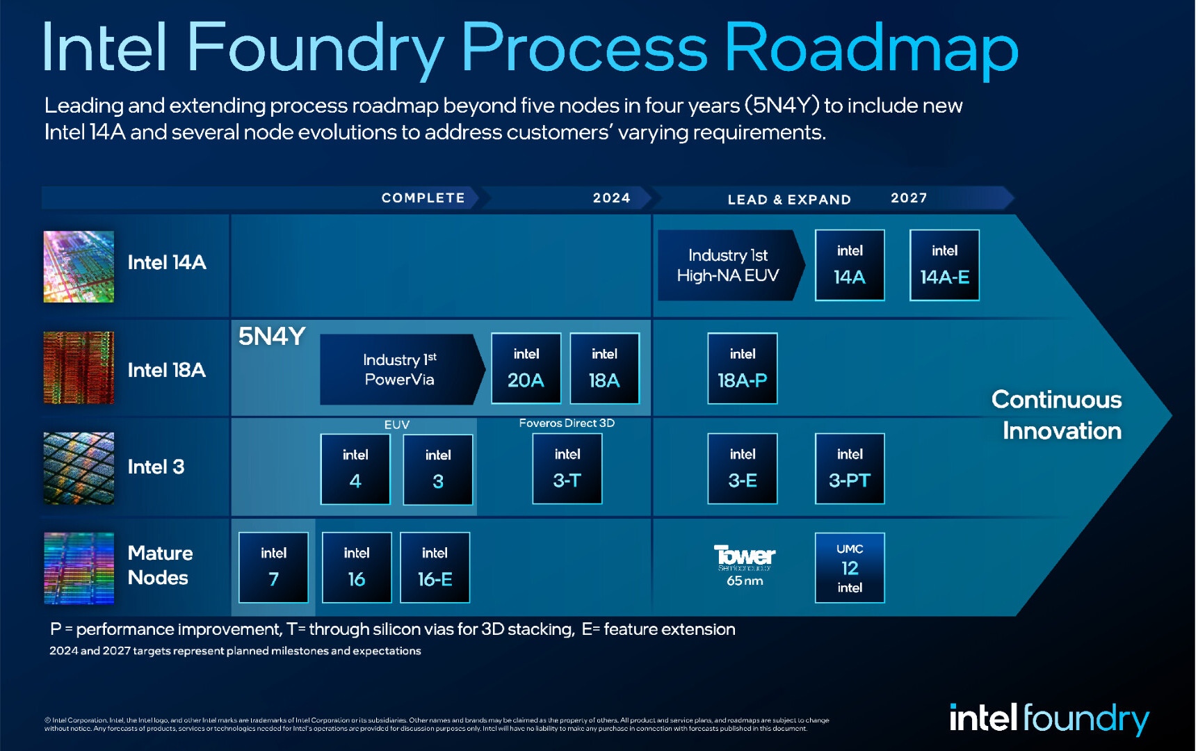
Process Roadmap Expands Beyond 5N4Y
Intel's extended process technology roadmap adds Intel 14A to the company's leading-edge node plan, in addition to several specialized node evolutions. Intel also affirmed that its ambitious five-nodes-in-four-years (5N4Y) process roadmap remains on track and will deliver the industry's first backside power solution. Company leaders expect Intel will regain process leadership with Intel 18A in 2025.
The new roadmap includes evolutions for Intel 3, Intel 18A and Intel 14A process technologies. It includes Intel 3-T, which is optimized with through-silicon vias for 3D advanced packaging designs and will soon reach manufacturing readiness. Also highlighted are mature process nodes, including new 12 nanometer nodes expected through the joint development with UMC announced last month. These evolutions are designed to enable customers to develop and deliver products tailored to their specific needs. Intel Foundry plans a new node every two years and node evolutions along the way, giving customers a path to continuously evolve their offerings on Intel's leading process technology.
Intel also announced the addition of Intel Foundry FCBGA 2D+ to its comprehensive suite of ASAT offerings, which already include FCBGA 2D, EMIB, Foveros and Foveros Direct.
Microsoft Design on Intel 18A Headlines Customer Momentum
Customers are supporting Intel's long-term systems foundry approach. During Pat Gelsinger's keynote, Microsoft Chairman and CEO Satya Nadella stated that Microsoft has chosen a chip design it plans to produce on the Intel 18A process.
"We are in the midst of a very exciting platform shift that will fundamentally transform productivity for every individual organization and the entire industry," Nadella said. "To achieve this vision, we need a reliable supply of the most advanced, high-performance and high-quality semiconductors. That's why we are so excited to work with Intel Foundry, and why we have chosen a chip design that we plan to produce on Intel 18A process."
Intel Foundry has design wins across foundry process generations, including Intel 18A, Intel 16 and Intel 3, along with significant customer volume on Intel Foundry ASAT capabilities, including advanced packaging.
In total, across wafer and advanced packaging, Intel Foundry's expected lifetime deal value is greater than $15 billion.
IP and EDA Vendors Declare Readiness for Intel Process and Packaging Designs
Intellectual property and electronic design automation (EDA) partners Synopsys, Cadence, Siemens, Ansys, Lorentz and Keysight disclosed tool qualification and IP readiness to enable foundry customers to accelerate advanced chip designs on Intel 18A, which offers the foundry industry's first backside power solution. These companies also affirmed EDA and IP enablement across Intel node families.
At the same time, several vendors announced plans to collaborate on assembly technology and design flows for Intel's embedded multi-die interconnect bridge (EMIB) 2.5D packaging technology. These EDA solutions will ensure faster development and delivery of advanced packaging solutions for foundry customers.
Intel also unveiled an "Emerging Business Initiative" that showcases a collaboration with Arm to provide cutting-edge foundry services for Arm-based system-on-chips (SoCs). This initiative presents an important opportunity for Arm and Intel to support startups in developing Arm-based technology and offering essential IP, manufacturing support and financial assistance to foster innovation and growth.
Systems Approach Differentiates Intel Foundry in the AI Era
Intel's systems foundry approach offers full-stack optimization from the factory network to software. Intel and its ecosystem empower customers to innovate across the entire system through continuous technology improvements, reference designs and new standards.
Stuart Pann, senior vice president of Intel Foundry at Intel said, "We are offering a world-class foundry, delivered from a resilient, more sustainable and secure source of supply, and complemented by unparalleled systems of chips capabilities. Bringing these strengths together gives customers everything they need to engineer and deliver solutions for the most demanding applications."
Global, Resilient, More Sustainable and Trusted Systems Foundry
Resilient supply chains must also be increasingly sustainable, and today Intel shared its goal of becoming the industry's most sustainable foundry. In 2023, preliminary estimates show that Intel used 99% renewable electricity in its factories worldwide. Today, the company redoubled its commitment to achieving 100% renewable electricity worldwide, net-positive water and zero waste to landfills by 2030. Intel also reinforced its commitment to net-zero Scope 1 and Scope 2 GHG emissions by 2040 and net-zero upstream Scope 3 emissions by 2050.
The announcements were made at Intel's first foundry event, Intel Foundry Direct Connect, where the company gathered customers, ecosystem companies and leaders from across the industry. Among the participants and speakers were U.S. Secretary of Commerce Gina Raimondo, Arm CEO Rene Haas, Microsoft CEO Satya Nadella, OpenAI CEO Sam Altman and others.
Process Roadmap Expands Beyond 5N4Y
Intel's extended process technology roadmap adds Intel 14A to the company's leading-edge node plan, in addition to several specialized node evolutions. Intel also affirmed that its ambitious five-nodes-in-four-years (5N4Y) process roadmap remains on track and will deliver the industry's first backside power solution. Company leaders expect Intel will regain process leadership with Intel 18A in 2025.
The new roadmap includes evolutions for Intel 3, Intel 18A and Intel 14A process technologies. It includes Intel 3-T, which is optimized with through-silicon vias for 3D advanced packaging designs and will soon reach manufacturing readiness. Also highlighted are mature process nodes, including new 12 nanometer nodes expected through the joint development with UMC announced last month. These evolutions are designed to enable customers to develop and deliver products tailored to their specific needs. Intel Foundry plans a new node every two years and node evolutions along the way, giving customers a path to continuously evolve their offerings on Intel's leading process technology.
Intel also announced the addition of Intel Foundry FCBGA 2D+ to its comprehensive suite of ASAT offerings, which already include FCBGA 2D, EMIB, Foveros and Foveros Direct.
Microsoft Design on Intel 18A Headlines Customer Momentum
Customers are supporting Intel's long-term systems foundry approach. During Pat Gelsinger's keynote, Microsoft Chairman and CEO Satya Nadella stated that Microsoft has chosen a chip design it plans to produce on the Intel 18A process.
"We are in the midst of a very exciting platform shift that will fundamentally transform productivity for every individual organization and the entire industry," Nadella said. "To achieve this vision, we need a reliable supply of the most advanced, high-performance and high-quality semiconductors. That's why we are so excited to work with Intel Foundry, and why we have chosen a chip design that we plan to produce on Intel 18A process."
Intel Foundry has design wins across foundry process generations, including Intel 18A, Intel 16 and Intel 3, along with significant customer volume on Intel Foundry ASAT capabilities, including advanced packaging.
In total, across wafer and advanced packaging, Intel Foundry's expected lifetime deal value is greater than $15 billion.
IP and EDA Vendors Declare Readiness for Intel Process and Packaging Designs
Intellectual property and electronic design automation (EDA) partners Synopsys, Cadence, Siemens, Ansys, Lorentz and Keysight disclosed tool qualification and IP readiness to enable foundry customers to accelerate advanced chip designs on Intel 18A, which offers the foundry industry's first backside power solution. These companies also affirmed EDA and IP enablement across Intel node families.
At the same time, several vendors announced plans to collaborate on assembly technology and design flows for Intel's embedded multi-die interconnect bridge (EMIB) 2.5D packaging technology. These EDA solutions will ensure faster development and delivery of advanced packaging solutions for foundry customers.
Intel also unveiled an "Emerging Business Initiative" that showcases a collaboration with Arm to provide cutting-edge foundry services for Arm-based system-on-chips (SoCs). This initiative presents an important opportunity for Arm and Intel to support startups in developing Arm-based technology and offering essential IP, manufacturing support and financial assistance to foster innovation and growth.
Systems Approach Differentiates Intel Foundry in the AI Era
Intel's systems foundry approach offers full-stack optimization from the factory network to software. Intel and its ecosystem empower customers to innovate across the entire system through continuous technology improvements, reference designs and new standards.
Stuart Pann, senior vice president of Intel Foundry at Intel said, "We are offering a world-class foundry, delivered from a resilient, more sustainable and secure source of supply, and complemented by unparalleled systems of chips capabilities. Bringing these strengths together gives customers everything they need to engineer and deliver solutions for the most demanding applications."
Global, Resilient, More Sustainable and Trusted Systems Foundry
Resilient supply chains must also be increasingly sustainable, and today Intel shared its goal of becoming the industry's most sustainable foundry. In 2023, preliminary estimates show that Intel used 99% renewable electricity in its factories worldwide. Today, the company redoubled its commitment to achieving 100% renewable electricity worldwide, net-positive water and zero waste to landfills by 2030. Intel also reinforced its commitment to net-zero Scope 1 and Scope 2 GHG emissions by 2040 and net-zero upstream Scope 3 emissions by 2050.
45 Comments on Intel Announces Intel 14A (1.4 nm) and Intel 3T Foundry Nodes, Launches World's First Systems Foundry Designed for the AI Era
(TPU article from 2018)
Hopefully Intel will be able to deliver on their plans and stay competitive. TSMC becoming a monopoly isn't good for us consumers.
TSMC 10 nm = 52 MTr / mm2
Intel 10 nm = 100.76 MTr / mm2
TSMC 7 nm = 114 MTr / mm2
TSMC 6 nm = 114 MTr / mm2
Intel 4 nm = 123 MTr / mm2
TSMC 5 nm = 138 MTr / mm2
TSMC 4 nm = 144 MTr / mm2
TSMC 3 nm = 224 MTr / mm2
TSMC 2 nm = 258 MTr / mm2intel/comments/15ctryl
Intel 3 nm = 133 MTr / mm2 ?
Intel 2 nm = ~150 MTr / mm2 ?
Intel 1.8 nm = 193 MTr / mm2 ?Don't forget SMIC, UMC, GlobalFoundries, Samsung and Intel.
If Zen 5 will use TSMC 4nm does Intel even stand a chance on a recovery in Q4 2024?
The other version is that Intel lacks engineering know-how to deliver anything beyond its 10nm/7 process. :rolleyes:Except that Intel has the larger pie of the market share, despite the very high competitiveness of Ryzen. That's only the DIY market and mostly in Germany which heavily favours AMD's products for historical reasons, they have a former AMD arm in Dresden?
www.statista.com/statistics/735904/worldwide-x86-intel-amd-market-share/
Samsung has not been able to score a huge client in recent years as far as I know. The last one was NVIDIA's consumer versions of Ampere - the datacenter version was made by TSMC.
Intel's process density isn't bad, the same goes for Samsung; the problem is that in terms of efficiency, both are crawling at the feet of TSMC
www.semianalysis.com/p/meteor-lake-die-shot-and-architecture
It's at an even greater 52% when you analyze the E core Crestmont. Analyzing individual blocks shows gains as much as 60% gains. L2 cache size has slightly decreased while capacity increased from 1.25 to 2MB, a 60% increase in density.Neither are TSMC's N3 3nm. After 32nm, meanings of process has been thrown out the window. Actually, deviation started back in 65-45nm.
It seems that people are still confused about Intel new naming scheme : it's a TSMC scale, intel 7nm is supposed to compete against TSMC 4nm hence they called it intel 4. ( And no, ADL/RPL being so inefficient isn't because intel 10nm doesn't in fact compete with TSMC 7nm, the arch is just inefficient vs AMD. Intel nodes were never comparable to the competition at equal number: TSMC 10nm was competing with Intel 14nm. They didn't care when they had the lead, but now they changed their naming to not look bad. That's a pure marketing strat. )
This should be better:
TSMC 10 nm = 52 MTr / mm2
Intel 10/7 nm = 100.76 MTr / mm2
TSMC 7 nm = 114 MTr / mm2
TSMC 6 nm = 114 MTr / mm2
TSMC 5 nm = 150 MTr / mm2
Intel 4 nm = 150 MTr / mm2
TSMC 4 nm = 155 MTr / mm2
TSMC 3 nm = 224 MTr / mm2
TSMC 2 nm = 258 MTr / mm2
Intel 3 nm = 160 MTr / mm2 ?
Intel 2 nm = ~180 MTr / mm2 ?
Intel 1.8 nm = 193 MTr / mm2 ?
No matter how accurate an analysis(or analyst) might be, unless they have insider info, they can't get it correct. Also, implementations are different. The 100 MTr/mm2 for Intel 10nm is also a theoretical value likely only reachable by certain sections of the chip such as graphics and their E cores. Their P cores never lived up to the post-22nm density claims with both 14nm and 10nm being 2x as dense rather than being 2.7x. Atom on the other hand got 64% reduction with 14nm Airmont, which is a 2.7x density gain and Tremont on 10nm is significantly smaller than Goldmont Plus at about 0.8-0.9mm2 or so despite the big changes.
Actually according to Intel, Intel 4 can reach 2x the density over Intel 7. In reality it doesn't, partly because full libraries won't be available until Intel 3. Same will be with 20A vs 18A. While 20A might sound impressive, it'll underperform(in perf and density) like Intel 4 and it'll be 18A that's good. There's a reason why the volume variants are coming only with Intel 3 and 18A. With 20A, it is a small subsection with current rumors saying it'll only come with 6+8 core for -S desktop Arrowlake and rest being on N3.
Another thing about Intel's 10nm implementations is that the high-performing versions such as the 10nm SF and the Intel 7 uses slightly larger pitch over the preceding variations. Intel 7 is slightly larger than 10nm SF, and 10nm SF over 10nm. Despite that, the die size did not change. However if they were to aim for max density, 10nm SF and Intel 7 would likely be a density reduction over 10nm. The E core on Alder/Raptor is at 1.5-1.7mm2 which is larger than expected and is a deviation and likely a combo of density reduction on Intel 7 plus needing to be stuck on larger cells due to being on the same process variant as the P core. Same seems true of Meteorlake with E core on that chip being 1mm2 when a near straight shrink should be smaller.
True picture is always much, much more complex than on the surface. Likely even if Intel reaches or even beats theoretical density on 18A over TSMC's N2, TSMC is still far more attractive to use because of the broad ecosystem support and reputation.
www.intc.com/news-events/press-releases/detail/1675/intel-launches-worlds-first-systems-foundry-designed-forIntel never mentioned 1.4nm in the press release. That was added by TPU :shadedshu:
Plus, there are things that do not scale any more. Memory is the most talked about one and one of the reasons AMD has been trying to get cache off to chiplets, be it 3DCache or MCD-s of RDNA3 GPUs.
We might want to differentiate between cache and actual memory such as RAM. RAM chips have been stuck under 1xnm(10-19nm) sizes for a decade now. The reason is because the simple structure of RAM means it's easier to scale, thus it hit tool limits faster, while things like SRAM in caches and logic are more complicated so it's further away from that. RAM cell sizes are fraction of SRAM, not just because of the 1T+1C vs 6T. Seriously, they are friggin' small! eDRAM, which is a variant for logic processes is few times smaller than SRAM, is few times larger than RAM cells.
SRAM is more complex, but it's still very regular structures easier to optimize, hence it hit the limit faster. Such limits disproportionately benefit companies that are behind, since they are further away from the limit. TSMC is the leader, so they hit it first. Intel was seriously behind, so Intel 4 is a 60% density gain for SRAM which is substantial. We'll see how Intel does once they become the leading edge.
Anyway 14nm wasn't great in the beggining, maybe not as bad as 10nm in the begining, but still far from being great.
Intel started production on 22n in 2012 but took them another 2 years before they were producing high quality chips. Ivy Bridge and Haswell refresh.
They started 14nm in 2014, but took them 3 years before they were producing high quality. Broadwel 2014 l and Coffee Lake 2017
The same with 10nm/Intel 7. 2018 Cannon Lake and 2022 Raptor Lake.
They were able to squeeze even more with Rocket Lake and Raptor Lake refresh.
So probably it will be the same with 7nm/Intel 4-3 in a few years they will yield great CPUs. And the same with 5nm Intel 20A 18A and later with 14A (3nm?).