News Posts matching #TGP

Return to Keyword Browsing

NVIDIA GeForce RTX 5090 and RTX 5080 Specifications Surface, Showing Larger SKU Segmentation

Thanks to the renowned NVIDIA hardware leaker kopite7Kimi on X, we are getting information about the final versions of NVIDIA's first upcoming wave of GeForce RTX 50 series "Blackwell" graphics cards. The two leaked GPUs are the GeForce RTX 5090 and RTX 5080, which now feature a more significant gap between xx80 and xx90 SKUs. For starters, we have the highest-end GeForce RTX 5090. NVIDIA has decided to use the GB202-300-A1 die and enabled 21,760 FP32 CUDA cores on this top-end model. Accompanying the massive 170 SM GPU configuration, the RTX 5090 has 32 GB of GDDR7 memory on a 512-bit bus, with each GDDR7 die running at 28 Gbps. This translates to 1,568 GB/s memory bandwidth. All of this is confined to a 600 W TGP.

When it comes to the GeForce RTX 5080, NVIDIA has decided to further separate its xx80 and xx90 SKUs. The RTX 5080 has 10,752 FP32 CUDA cores paired with 16 GB of GDDR7 memory on a 256-bit bus. With GDDR7 running at 28 Gbps, the memory bandwidth is also halved at 784 GB/s. This SKU uses a GB203-400-A1 die, which is designed to run within a 400 W TGP power envelope. For reference, the RTX 4090 has 68% more CUDA cores than the RTX 4080. The rumored RTX 5090 has around 102% more CUDA cores than the rumored RTX 5080, which means that NVIDIA is separating its top SKUs even more. We are curious to see at what price point NVIDIA places its upcoming GPUs so that we can compare generational updates and the difference between xx80 and xx90 models and their widened gaps.

NVIDIA RTX 5090 "Blackwell" Could Feature Two 16-pin Power Connectors

NVIDIA CEO Jensen Huang never misses an opportunity to remind us that Moore's Law is cooked, and that future generations of logic hardware will only get larger and hotter, or hungrier for power. NVIDIA's next generation "Blackwell" graphics architecture promises to bring certain architecture-level performance/Watt improvements, coupled with the node-level performance/Watt improvements from the switch to the TSMC 4NP (4 nm-class) node. Even so, the GeForce RTX 5090, or the part that succeeds the current RTX 4090, will be a power hungry GPU, with rumors suggesting the need for two 16-pin power inputs.

TweakTown reports that the RTX 5090 could come with two 16-pin power connectors, which should give the card the theoretical ability to pull 1200 W (continuous). This doesn't mean that the GPU's total graphics power (TGP) is 1200 W, but a number close to or greater than 600 W, which calls for two of these connectors. Even if the TGP is exactly 600 W, NVIDIA would want to deploy two inputs, to spread the load among two connectors, and improve physical resilience of the connector. It's likely that both connectors will have 600 W input capability, so end-users don't mix up connectors should one of them be 600 W and the other keyed to 150 W or 300 W.

AMD Intros Radeon RX 7800M Mobile Graphics Based on "Navi 32" Silicon

AMD officially launched the Radeon RX 7800M mobile graphics, which fills the rather vast gap that exists between its flagship Radeon RX 7900M, and the mid-range RX 7600M XT. This is the first official outing of the "Navi 32" GPU on the mobile platform. The RX 7800M maxes out the "Navi 32," enabling all 60 compute units, however, it does not max out the memory bus. The RX 7800M comes with 12 GB of 18 Gbps GDDR6 memory across a 192-bit wide memory bus. This means that only three out of four memory cache dies (MCDs) of the "Navi 32" are enabled, giving the chip 48 MB of Infinity Cache.

The RX 7800M essentially has the GCD core configuration of the desktop RX 7800 XT, but with the memory and cache configuration of the desktop RX 7700 XT. The 60 CU give it 3,840 stream processors, 120 AI accelerators, 60 ray accelerators, 240 TMUs, and 96 ROPs. The GPU comes with a Game Clocks frequency of 2145 MHz, while the memory ticks at 18 Gbps (432 GB/s memory bandwidth). AMD has given the RX 7800M a total graphics power (TGP) value of 180 W, which makes it fit for performance-segment gaming notebooks and mobile workstations. For reference, the RX 7900M comes with a TGP range of 180-200 W.

NVIDIA Testing GeForce RTX 50 Series "Blackwell" GPU Designs Ranging from 250 W to 600 W

According to Benchlife.info insiders, NVIDIA is supposedly in the phase of testing designs with various Total Graphics Power (TGP), running from 250 Watts to 600 Watts, for its upcoming GeForce RTX 50 series Blackwell graphics cards. The company is testing designs ranging from 250 W aimed at mainstream users and a more powerful 600 W configuration tailored for enthusiast-level performance. The 250 W cooling system is expected to prioritize compactness and power efficiency, making it an appealing choice for gamers seeking a balance between capability and energy conservation. This design could prove particularly attractive for those building small form-factor rigs or AIBs looking to offer smaller cooler sizes. On the other end of the spectrum, the 600 W cooling solution is the highest TGP of the stack, which is possibly only made for testing purposes. Other SKUs with different power configurations come in between.

We witnessed NVIDIA testing a 900-watt version of the Ada Lovelace AD102 GPU SKU, which never saw the light of day, so we should take this testing phase with a grain of salt. Often, the engineering silicon is the first batch made for the enablement of software and firmware, while the final silicon is much more efficient and more optimized to use less power and align with regular TGP structures. The current highest-end SKU, the GeForce RTX 4090, uses 450-watt TGP. So, take this phase with some reservations as we wait for more information to come out.

US Government Wants Nuclear Plants to Offload AI Data Center Expansion

The expansion of AI technology affects not only the production and demand for graphics cards but also the electricity grid that powers them. Data centers hosting thousands of GPUs are becoming more common, and the industry has been building new facilities for GPU-enhanced servers to serve the need for more AI. However, these powerful GPUs often consume over 500 Watts per single card, and NVIDIA's latest Blackwell B200 GPU has a TGP of 1000 Watts or a single kilowatt. These kilowatt GPUs will be present in data centers with 10s of thousands of cards, resulting in multi-megawatt facilities. To combat the load on the national electricity grid, US President Joe Biden's administration has been discussing with big tech to re-evaluate their power sources, possibly using smaller nuclear plants. According to an Axios interview with Energy Secretary Jennifer Granholm, she has noted that "AI itself isn't a problem because AI could help to solve the problem." However, the problem is the load-bearing of the national electricity grid, which can't sustain the rapid expansion of the AI data centers.

The Department of Energy (DOE) has been reportedly talking with firms, most notably hyperscalers like Microsoft, Google, and Amazon, to start considering nuclear fusion and fission power plants to satisfy the need for AI expansion. We have already discussed the plan by Microsoft to embed a nuclear reactor near its data center facility and help manage the load of thousands of GPUs running AI training/inference. However, this time, it is not just Microsoft. Other tech giants are reportedly thinking about nuclear as well. They all need to offload their AI expansion from the US national power grid and develop a nuclear solution. Nuclear power is a mere 20% of the US power sourcing, and DOE is currently financing a Holtec Palisades 800-MW electric nuclear generating station with $1.52 billion in funds for restoration and resumption of service. Microsoft is investing in a Small Modular Reactors (SMRs) microreactor energy strategy, which could be an example for other big tech companies to follow.

NVIDIA's China-only GeForce RTX 4090D Launched with Fewer Shaders than Regular RTX 4090

NVIDIA today formally launched the China-specific GeForce RTX 4090D graphics card for gaming and creator applications, after it was banned this October by the United States Federal Trade Commission from exporting the RTX 4090 (among other AI GPUs) to China. The RTX 4090D comes with a reduced AI inference performance than the RTX 4090 to comply with the US-FTC limits, and measures are put in place to prevent end-users from modifying it into a regular RTX 4090. Besides firmware and driver-level performance limiters, the card gets a completely different ASIC code, a different device ID (which prevents BIOS transplants from the RTX 4090); and a different core-configuration of the 5 nm "AD102" silicon itself.

The "AD102" silicon physically has 72 TPCs (144 SM), from which NVIDIA carved out the original RTX 4090 by enabling 64 TPCs (128 SM). The new RTX 4090D only gets 57 TPCs (114 SM), which reduces the counts of the CUDA cores, Tensor cores, and RT cores. While the original RTX 4090 has 16,384 CUDA cores, 512 Tensor cores, and 128 RT cores; the new RTX 4090D is configured with 14,592 CUDA cores, 456 Tensor cores, and 114 RT cores. The GPU clocks are the same, both boost up to 2.52 GHz, although the power limits are reduced, with the TGP lowered by 25 W. The memory sub-system appears untouched. We are also hearing that overclocking of the RTX 4090D will be limited, with lower slider limits—all to prevent end-users from regaining AI inference performance levels comparable to an RTX 4090. NVIDIA is pricing the RTX 4090D at a baseline price of RMB ¥12,999 ($1,840), which was the launch price of the original RTX 4090 in China, before it was scalped out of existence there.

Intel Launches Mobile Arc A570M and A530M

Without fanfare, Intel has launched two new mobile GPUs in the shape of the Arc A570M and the A530M. The Arc A570M gets 16 Xe Cores and 256 execution units, as well as four render slices and 16 RT units. The lower-end Arc A530M gets to make do with 12 Xe cores, 192 execution units, three render slices and 12 RT units, which is a smaller cut than the model name suggests. What's interesting to note here is that the Arc A570M appears to have identical hardware specs to the Arc A550M that launched in the second quarter of 2022, although as we'll see, the clock speeds and TGP differ between the parts. The Arc A570M supports 8 GB of GDDR6 memory, the same as the Arc A550M, with the Arc A530M supports 4 or 8 GB of GDDR6.

Both the Arc A570M and the A530M will get a GPU clock speed of 1,300 MHz, which is a significant boost from the Arc A550M which is plodding along at a mere 900 MHz in comparison. This makes the two newcomers Intel's third highest clocked mobile GPUs, with only the Arc A770M and Arc A370M being clocked higher. The downside of this is an increase in TGP, where the Arc A550M had a fairly reasonable TGP of 60 Watts, the Arc A530M has a TGP range of 65 to 95 Watts, while the Arc A570M extends this to 75-95 Watts. The rest of the specs appear to carry over from the Arc A550M, so the new GPUs will support up to four displays via eDP, DP 2.0 or HDMI 2.1 and the full set of video encoders and decoders are also supported. The new additions are still made using TSMC's N6 node, so what we're looking at are most likely just optimised silicon here, which has led Intel to be able to boost the clock speeds while maintaining acceptable thermals.

NVIDIA AD107 Silicon Powering GeForce RTX 4060 Pictured

The "AD107" is expected to be the smallest client GPU based on the NVIDIA "Ada Lovelace" graphics architecture. The upcoming GeForce RTX 4060 (non-Ti) is rumored to be maxing this silicon out (enabling all available shaders). MEGAsizeGPU scored one of the first pictures of the "AD107" in the flesh, revealing a small fiberglass substrate, and a visibly smaller die than the "AD106" powering the RTX 4060 Ti.

The "AD107" silicon is expected to feature 3,072 CUDA cores across 24 SM (streaming multiprocessors). The GPU features a 128-bit wide memory interface much like the "AD106," and NVIDIA is expected to use conventional 17 Gbps GDDR6 memory, which works out to 272 GB/s memory bandwidth. 8 GB is the standard memory size for the RTX 4060. With "Ada," NVIDIA has rebalanced the memory sub-system with greater reliance on on-die caches, and the "AD107" features a 24 MB L2 cache. Much like the "AD106," the smaller "AD107" features a PCI-Express 4.0 x8 host interface. The ace up its sleeve has to be power, with even the maxed out RTX 4060 only being rated for 119 W of TGP.

Pictures of the Never-Released RTX 4070 Ti Founders Edition, RTX 4060 Ti Founders Edition, and RTX 4060 Founders Edition Emerge

When NVIDIA got around to release the $800 GeForce RTX 4070 Ti "Ada" (originally meant to launch as the RTX 4080 12 GB); an NVIDIA Founders Edition product based on this chip was conspicuous in its absence. A tech enthusiast who goes by "KittyYYuko" on Twitter posted pictures of what they claim to be the never-released RTX 4070 Ti Founders Edition; and upcoming RTX 4060 Ti and RTX 4060. The claim begins to check out as we're shown a picture of a graphics card PCB with the distinct Founders Edition shape, which has an "AD104" ASIC, and a 16-pin 12VHPWR connector, along with 8 memory pads, two of which are unoccupied (matches the 192-bit memory interface of the RTX 4070 Ti).

We are shown two other cards, the RTX 4060 Ti Founders Edition, and the RTX 4060 Founders Edition. These are expected to be positioned below the RTX 4070 that the company plans to launch in April. The Founders Edition boards are visibly smaller than even the RTX 3080 Founders Edition, although they stick to the dual-axial flow-through design of that card. "AD106" based graphics cards are expected to have typical graphics power (TGP) values well under the 250 W-mark, for which this cooler looks adequate, considering that the sheet-metal of the heatsink has been pushed to the very edges of the card. The cards could include power adapters that convert no more than two 8-pin PCIe to a 16-pin 12VHPWR with a 300 W power limit.

XMG Introduces PRO and FOCUS Laptops with i9-13900HX and RTX 4070

With the new PRO and the FOCUS (E23), XMG introduces two laptop series on a similar hardware basis: Both feature Intel's Core i9-13900HX and NVIDIA graphics cards up to the GeForce RTX 4070. While the PRO 15 and PRO 17 are slightly thinner as gaming workstations and boast more extensive connectivity, the FOCUS scores at a more affordable price and is not only available in 15.6 and 17.3-inch versions, but also in a 16-inch format. For the laptops originally designed as an entry-level series, the hardware upgrades mean a significant upgrade: the FOCUS series moves closer to the PRO laptops.

The key components found in the new XMG PRO 15 and PRO 17 as well as the XMG FOCUS 15, FOCUS 16 and FOCUS 17 are almost identical. All laptops employ Intel's Core i9-13900HX with 24 cores (8 P-cores, 16 E-cores) and 32 threads. The freely configurable graphics card options each include NVIDIA's new, DLSS-3-capable GeForce RTX 4050 (FOCUS only) as well as 4060 and 4070 (FOCUS and PRO) with a maximum graphics power rating of up to 140 watts (115 watts TGP plus 25 watts Dynamic Boost 2.0). However, since the clock behaviour and the actual power consumption of the GPUs in the new generation are subject to much more restrictive, application-specific specifications from NVIDIA, the maximum values are only achieved in synthetic stress tests such as Furmark - according to the official requirements of the graphics chip manufacturer.

NVIDIA GeForce RTX 40 Series "AD104" Could Match RTX 3090 Ti Performance

NVIDIA's upcoming GeForce RTX 40 series Ada Lovelace graphics card lineup is slowly shaping up to be a significant performance uplift compared to the previous generation. Today, according to a well-known hardware leaker kopite7kimi, we are speculating that a mid-range AD104 SKU could match the performance of the last-generation flagship GeForce RTX 3090 Ti graphics card. The full AD104 SKU is set to feature 7680 FP32 CUDA cores, paired with 12 GB of 21 Gbps GDDR6X memory running on a 192-bit bus. Coming with a large TGP of 400 Watts, it should have a performance of the GA102-350-A1 SKU found in GeForce RTX 3090 Ti.

Regarding naming this complete AD104 SKU, it should end up as a GeForce RTX 4070 Ti model. Of course, we must wait and see what NVIDIA decides to do with the lineup and what the final models will look like.

NVIDIA RTX 40 Series Could Reach 800 Watts on Desktop, 175 Watt for Mobile/Laptop

Rumors of NVIDIA's upcoming Ada Lovelace graphics cards keep appearing. With every new update, it seems like the total power consumption is getting bigger, and today we are getting information about different SKUs, including mobile and desktop variants. According to a well-known leaker, kopite7kimi, we have information about the power limits of the upcoming GPUs. The new RTX 40 series GPUs will feature a few initial SKUs: AD102, AD103, AD104, and AD106. Every SKU, except the top AD102, will be available as well. The first in line, AD102, is the most power-hungry SKU with a maximum power limit rating of 800 Watts. This will require multiple power connectors and a very beefy cooling solution to keep it running.

Going down the stack, we have an AD103 SKU limited to 450 Watts on desktop and 175 Watts on mobile. The AD104 chip is limited to 400 Watts on desktop, while the mobile version is still 175 Watts. Additionally, the AD106 SKU is limited to 260 Watts on desktop and 140 Watts on mobile.

Sapphire Radeon RX 6950X TOXIC Reportedly Boosts to 2565 MHz at 346W TGP

As AMD is preparing to launch a highly-anticipated refresh of the Radeon RX 6000 series, codenamed RX 6x50 XT series. Alongside AMD, add-in board partners (AIBs) will have their say as well, and today we get to take a look at the alleged specifications of Sapphire's highest-end upcoming products. According to Chiphell member RaulMee, who claims to possess the specification of the newest Sapphire models, we are expected to see a bit higher total board power (TGP) with the arrival of this refresh. First and foremost, the Sapphire RX 6950XT TOXIC is the fastest air-cooled model from Sapphire, with a boost clock of up to 2565 MHz (255 MHz over AMD's reference 2310 MHz model), carrying a TGP of 364 Watts in OC BIOS. Regular TGP for this model is 332 Watts with a boost speed of up to 2532 MHz. Please note that this includes the power output of GPU and memory.

Next up, we have Sapphire's RX 6950XT NITRO+ SKUs. The non-SE card is a minor improvement over the AMD Radeon RX 6950XT reference GPU and offers a Silent BIOS option. The RX 6950XT NITRO+ Special Edition can go up to 325 Watts and 2435 MHz with OC BIOS applied. Silent BIOS is also an option, and it lowers the TGP to 303 Watts and 2368 MHz. The alleged specification chart also carries Sapphires' RX 6750XT & 6650XT NITRO+ GPUs, of which you can check the clock speeds and TGPs below.
NVIDIA Allegedly Testing a 900 Watt TGP Ada Lovelace AD102 GPU

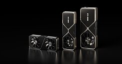
With the release of Hopper, NVIDIA's cycle of new architecture releases is not yet over. Later this year, we expect to see next-generation gaming architecture codenamed Ada Lovelace. According to a well-known hardware leaker for NVIDIA products, @kopite7kimi, on Twitter, the green team is reportedly testing a potent variant of the upcoming AD102 SKU. As the leak indicates, we could see an Ada Lovelace AD102 SKU with a Total Graphics Power (TGP) of 900 Watts. While we don't know where this SKU is supposed to sit in the Ada Lovelace family, it could be the most powerful, Titan-like design making a comeback. Alternatively, this could be a GeForce RTX 4090 Ti SKU. It carries 48 GB of GDDR6X memory running at 24 Gbps speeds alongside monstrous TGP. Feeding the card are two 16-pin connectors.

Another confirmation from the leaker is that the upcoming RTX 4080 GPU uses the AD103 SKU variant, while the RTX 4090 uses AD102. For further information, we have to wait a few more months and see what NVIDIA decides to launch in the upcoming generation of gaming-oriented graphics cards.

NVIDIA GeForce RTX 3080 Ti Mobile Brings 16 Gbps Memory and TGP of 175 Watts

NVIDIA is preparing to launch an ultimate solution for high-end laptops and gamers that could benefit from the high-performance graphics card integration in mobile systems like gaming laptops. Rumored to launch sometime in January, NVIDIA is preparing a GeForce RTX 3080 Ti mobile GPU SKU that supposedly offers the highest performance in the Ampere mobile family. According to sources close to VideoCardz, team green has prepared to announce RTX 3080 Ti mobile design with faster memory and higher total graphics power (TGP). The memory speed will get an upgrade to 16 Gbps, compared to the 14 Gbps speed in RTX 3080 mobile SKU.

Similarly, the total overall TGP will also receive a bump to 175 Watts. This is just a tad higher than the 165 Watt TGP of RTX 3080 mobile. The Ti version will upgrade the CUDA core count and other things like TMUs to undetermined specifications. Currently, it is rumored that the Ti version could carry 7424 CUDA cores, which is an upgrade from 6144 of the regular RTX 3080 version.

Acer Offers Increased Laptop GPU Performance Using Firmware Update

Total Graphics Power, or TGP, is a way of constraining the power of a GPU to a certain level, so it can adjust to the use case. In laptops and other mobile systems, TGP can be dynamically adjusted using technologies such as NVIDIA Dynamic Boost and AMD Smart Shift, which bring unused CPU power envelope to the GPU and allowing it to boost to much higher frequencies. By boosting to higher frequencies, the total power output of GPU increased, and the cooling system of a laptop can only handle a limited amount of heat. That is why these technologies from AMD and NVIDIA allow the CPU to reduce its heat output and offer the GPU more room for boosting and power output.

Acer has today announced that the company will offer a simple firmware update for their Nitro 5, Helios 300, Triton 300, and Triton 300 SE gaming laptops, which is going to boost the TGP of NVIDIA graphics card present in these systems anywhere from 5-30 Watts. There is a nicely compiled list available on the ComputerBase website that highlights the exact power increase for a specific model. If you happen to own one of these models, you can download the latest firmware update from Acer's website here.

HP Unleashes OMEN 16/17 Gaming Laptops and Customizable OMEN 25i Gaming Monitor

HP introduced its latest gaming hardware and software designed for today's gamers with the powerful OMEN 16 and OMEN 17, bright and customizable OMEN 25i Gaming Monitor, and community gaming with OMEN OASIS Beta feature in OMEN Gaming Hub. The company also debuted Victus by HP, its next-generation mainstream-level gaming PC portfolio, with a 16-inch laptop.

Gaming continues to be an outlet for entertainment and connecting with friends. Two out of three people are spending more time watching videos and gaming than they did prior to the pandemic, with one in four gaming three to four hours more and almost one in five gaming six to ten hours more a week6. HP's next-generation gaming portfolio is designed for both veteran gamers and enthusiast explorers to be entertained, connected, and empowered to progress in their favorite games.

AMD Radeon RX 6600 Series to Feature PCIe 4.0 x8 Interface and up to 8 GB of GDDR6 Memory

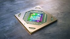
German publication, Igor's LAB, has got ahold of some information regarding AMD's upcoming Radeon RX 6600 series graphics card. Based on the Navi 23 SKU, the GPU is supposed to satisfy all the entry-level needs one would expect from a GPU. That means light 1080p gaming and multimedia streaming. For starters, let's get into details of the die. Igor's LAB notes that the die size is 235.76mm2, with a 35x35 mm package. The die will be centered in a package with a 45-degree rotation, which you can see how it looks in the images below. Additionally, the Navi 23 GPU will have SKUs ranging from 65 Watts to 95 Watts of Total Graphics Power (TGP). As far as frequency goes, the card BIOS points to the maximum clock speed of 2350 MHz, which is lower than the rumored 2684 MHz.
When it comes to memory, the upcoming Navi 23 GPUs can be equipped with up to 16 GB of GDDR6 memory, however, it is most likely that the regular gamer version will come with 8 GB of VRAM, while the Radeon Pro models will use the full 16 GB limit. As far as interface is concerned, the Radeon RX 6600 series will be limited to PCIe 4.0 x8 connection, as the low-end GPU doesn't require a full x16 slot. With the bandwidth of the PCIe 4.0, only eight lanes are enough for this GPU. These cards are expected to hit the market sometime in June, and we are waiting for the official announcement.

Intel Xe-HPG DG2 GPU Specifications Leak, First GPUs are Coming in H2 2021 in Alder Lake-P Laptops

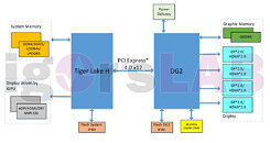
Yesterday, we got information that Intel's upcoming DG2 discrete graphics card is "right around the corner". That means that we are inching closer to the launch of Intel's discrete GPU offerings, and we are going to get another major player in the current GPU market duopoly. Today, however, we are in luck because Igor from Igor's LAB has managed to get ahold of the specifications of Intel's Xe-HPG DG2 graphics card. For starters, it is important to note that DG2 GPU will first come to laptops later this year. More precisely, laptops powered by Alder Lake-P processors will get paired with DG2 discrete GPU in the second half of 2021. The CPU and GPU will connect using the PCIe 4.0 x12 link as shown in the diagram below, where the GPU is paired with the Tiger Lake-H processor. The GPU has its subsystem that handles the IO as well.

Lenovo Teases NVIDIA GeForce RTX 3050 and RTX 3050 Ti Clock Speeds and TGP

NVIDIA is preparing the launch of an entry-level graphics card based on the Ampere architecture, sometimes later in the year, with possible dates being this or the following quarter. The GeForce RTX 3050 and RTX 3050 Ti are supposed to be the slowest SKUs in the whole Ampere lineup, representing the least expensive choice from the entire generation. However, we are wondering what the cards will look like and what are some design choices NVIDIA will introduce to these SKUs. Lenovo, the maker of the popular various kinds of laptops, has accidentally listed these exact SKUs in the specification section of its Legion gaming laptop.

The GPUs in question are NVIDIA GeForce RTX 3050 and RTX 3050 Ti mobile edition SKUs, probably based on the GA107 GPU SKU. Both versions are equipped with 4 GB of GDDR6 memory running on a 128-bit bus. The regular GeForce RTX 3050 SKU is configurable from a TGP of just 60 to 80 Watts. NVIDIA has a Dynamic Boost technology that will pump that by additional 15 Watts and max it out at 95 Watt SKU, which this laptop uses. The maximum boost clock frequency of these cards is 1695 MHz and 1740 MHz, for the RTX 3050 Ti and RTX 3050 GPUs respectively.

ASUS ROG Zephyrus Duo 15 Owners are Applying Custom GPU vBIOS with Higher TGP Presets

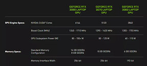
With NVIDIA's GeForce RTX 30-series lineup of GPUs, laptop manufacturers are offered a wide variety of GPU SKUs that internally differ simply by having different Total Graphics Power (TGP), which in turn results in different clock speeds and thus different performance. ASUS uses NVIDIA's variant of GeForce RTX 3080 mobile GPU inside the company's ROG Zephyrus Duo (GX551QS) with a TGP of 115 Watts, and Dynamic Boost technology that can ramp up the card to 130 Watts. However, this doesn't represent the maximum for RTX 3080 mobile graphics card. The maximum TGP for RTX 3080 mobile goes up to 150 Watts, which is a big improvement that lets the GPU reach higher frequencies and more performance.

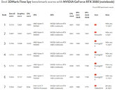
Have you ever wondered what would happen if you manually applied vBIOS that allows the card to use more power? Well, Baidu forum users are reporting a successful experiment of transforming their 115 W RTX 3080 to 150 W TGP card. Using GPU vBIOS from MSI Leopard G76, which features a 150 W power limit, and applying it to the ROG's Zephyrus Duo power-limited RTX 3080 cards is giving results. Users have successfully used this vBIOS to squeeze out more performance from their laptops. As seen on the 3D Mark Time Spy rank list, the entries are now dominated solely by modified laptops. Performance improvement is, of course, present and it reaches up to a 20% increase.

In a Bid for Transparency, NVIDIA Requires Laptop Manufacturers to List GPU Specs for RTX 3000 Series

It seemed has if NVIDIA was dropping the Max-P and Max-Q differentiators for their mobile graphics card, which would throw consumers into disarray and confusion as to what exactly was the performance of the graphics card built into their RTX 30-series laptop. In essence, due to the RTX 30-series configurable TGP (Total Graphics Power), as well as each laptop's own capability of supplying power and cooling to that chip, users might see themselves in situations such as their mobile RTX 3080 offering lower performance than a mobile RTX 3070, configured for a higher TGP. This meant that more attentive users would have to hunt for reviews of the laptops they were eyeing, or to be forced to count on system manufacturers to actually list specifications for the included graphics solution in their laptops. This would mean, more often than not, something akin to chaos, and could in truth impact NVIDIA's brand recognition and consumer confidence in expected performance.

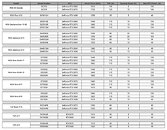
NVIDIA, as a way to circumvent this, has decided to not only encourage, but actually require that manufacturers list their graphics cards' TGP as well as specific clock speed stats on their online product pages. Some manufacturers, such as Asus, Acer, Razer, Origin, MSI, Alienware, and Gigabyte have already updated some product pages - but not all. An NVIDIA spokesperson clarified to The Verge that "We're requiring OEMs to update their product pages to the Max-Q technology features for each GeForce laptop, as well as clocks and power — which communicates the expected GPU performance in that system." Perhaps that will help consumers make a more informed decision.
NVIDIA reference specs example ASUS Laptop TGP Listing
Return to Keyword Browsing
Oct 6th, 2024 12:46 EDT change timezone

New Forum Posts

Popular Reviews

Controversial News Posts