
News Posts matching #Zen 7

Return to Keyword Browsing

AMD Zen 7 "Grimlock" APUs to Feature New RDNA 5+ Graphics in 2029, Leaker Claims

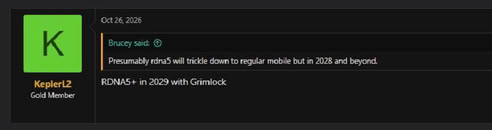
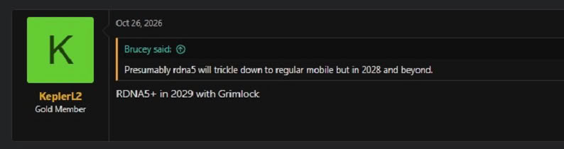
Leaker Kepler_L2 says AMD will bring RDNA 5+ to its Zen 7 "Grimlock" APUs in 2029. He posted on the NeoGAF forum, replying to a user who guessed RDNA 5 would trickle down to regular mobile chips in 2028 or later. His answer was "RDNA5+ in 2029 with Grimlock." He gave no details on how RDNA 5+ differs from RDNA 5, and AMD hasn't confirmed the name or timing. Grimlock is the codename for the Zen 7 Ryzen generation. This update follows Kepler_L2's January claim that AMD is splitting its APU roadmap in two. Products that don't need strong integrated graphics, like office laptops or laptops with a high-end discrete GPU, stay on RDNA 3.5 until 2029, while "premium" parts get RDNA 5. Medusa Halo is expected to be one of those.

The picture is messy, though. We previously reported that Medusa Point should get RDNA 4m, a tweaked RDNA 3.5 with FSR 4 support, and AMD's HIPRT 3.2 release notes list Medusa support for gfx1170, gfx1171 and gfx115E. The gfx115x family is RDNA 3.5, so it looks like at least one Medusa chip could stick with it. If this ends up being true, anyone waiting on a mainstream Ryzen laptop or handheld with RDNA 5 graphics may be waiting a long time. That's a long run for one iGPU architecture, but of course, this is all leak territory until AMD says something concrete.
AMD "Zen 7" IP to Use TSMC A14 Node and More Advanced Packaging

AMD is gradually preparing to launch its next-generation "Zen 6" series of processors under the new EPYC "Venice" server CPU family. Meanwhile, development of the "Zen 7" architecture has been ongoing for quite some time, and it seems we are finally learning which manufacturing node AMD will use for this CPU generation. According to Taiwanese media outlet Commercial Times, AMD is reportedly considering TSMC's A14 node, officially utilizing the first angstrom-era node for its products. As readers may recall, AMD recently began high-volume production of its EPYC "Venice" on the 2 nm node, but with the upcoming "Zen 6" architecture. We have covered the advancements that "Zen 6" brings over the current "Zen 5," but the next-generation "Zen 7" is expected to elevate performance to a whole new level, especially with the power and performance enhancements of the new TSMC A14 node.

For "Zen 7" CCD IP codenamed "Grimlock," AMD plans to make its CPU architecture more AI-relevant, allowing future processing workloads to better leverage the processing power of 16 CPU cores per CCD. Among the key features are AVX10 and ACE. AVX10 unifies AVX-512 and AVX2 features to improve performance and compatibility across vector math-heavy workloads. ACE, or Advanced Matrix Extensions for Matrix Manipulation, is an industry-standard matrix math instruction set that could be relevant to a wide range of devices, from smartphones to servers. Other ISA additions with "Zen 7" include FRED (Flexible Return and Event Delivery), which replaces the current device interrupt model to reduce system-level latency. "Zen 7" also implements ChkTag x86 Memory Tagging to counteract various memory-level data vulnerabilities caused by buffer overflows and use-after-free errors.

AMD to Expand EPYC Lineup With Specialized CPUs for AI, HPC, and Cloud

AMD's CPU offerings will soon expand into more categories, specializing in different tasks and use cases. During the latest Q1 earnings call, AMD CEO Dr. Lisa Su confirmed that customers are increasingly interested in specialized EPYC solutions and that future CPU generations will cater to different customer needs. This means that agentic AI will receive a dedicated EPYC CPU SKU, HPC workloads will have their own EPYC CPU SKU, AI training and inference will get a separate EPYC SKU, and cloud workloads will have a distinct SKU. This expansion of task-specialized CPU designs will go beyond the "Venice" CPU platform, which is expected to be released this year. At CES 2026, AMD confirmed that EPYC "Venice" will be a highly dense CPU package with up to 256 cores and 512 threads of "Zen 6c" cores, while the regular "Zen 6" configuration will have a maximum of 96 cores and 192 threads.

With this generation of EPYC CPUs based on the "Zen 6" core IP, AMD will promote "Venice" CPUs broadly, while the "Venice" CPU generation will be complemented by the "Verano" CPUs. These appear to use the same "Zen 6" microarchitecture but have optimizations specifically designed for AI infrastructure. Contrary to previous assumptions that "Verano" would be a "Zen 7" IP, it is now confirmed to be part of the 6th-generation EPYC CPU family. This indicates that AMD is starting its CPU customization for different workloads as early as this year. As the server CPU market is projected to reach $120 billion by the end of this decade, less than 3.5 years away in 2030, it makes sense to have different CPU SKUs for each task and capture a significant portion of that revenue. Server CPUs are also expected to grow at a 35% compound annual growth rate, which is impressive for a relatively mature market.

AMD Zen 7 to Implement AVX10 and ACE Instruction Sets

AMD on Tuesday unveiled its future "Zen 7" CPU microarchitecture. The company has been pivoting toward making its CPU IP more AI-relevant, so future processing workloads could better leverage the serial processing power of CPUs. Among these, the two important ones are AVX10 and ACE. AVX10 sees a unification of AVX-512 and AVX2 features to improve performance and compatibility across vector math heavy workloads. ACE, or Advanced Matrix Extensions for Matrix Manipulation, is an industry-standard matrix math instruction set that could prove to be relevant to every device ranging from smartphones to servers.

Among the other ISA additions with Zen 7 are FRED (flexible return and event delivery), which replaces the current device interrupt model to reduce system-level latency. Zen 7 also implements ChkTag x86 Memory Tagging to counteract several kinds of memory-level data vulnerabilities caused by buffer overflows and use-after-free errors. FRED in particular was a noteworthy feature Intel was working on for its x86S machine architecture standard.

AMD Confirms Zen 6 (2 nm) and Zen 7 with Efficiency Upgrades and New AI Features

AMD has updated its CPU core roadmap confirming Zen 6 and Zen 7 architectures as the next steps for its Ryzen and EPYC product families. The new roadmap was shown during the company's Financial Analyst Day 2025. Zen 6 will launch next year and is built using TSMC's 2 nm process node. The lineup will include both Zen 6 and Zen 6C variants, optimized respectively for high performance and power efficiency. According to AMD CTO Mark Papermaster, Zen 6 will bring higher IPC, improved efficiency and expanded AI data type support with additional AI pipelines. We recently detailed here the first Zen 6 ISA changes, which introduce several new instruction sets and expanded compute capabilities. The architecture will appear across multiple platforms, including EPYC "Venice," Ryzen Desktop "Olympic Ridge," and Ryzen Mobile "Medusa Point."

For the first time, AMD has also confirmed Zen 7, listed on the roadmap as a "Future Node" and "Next-Generation" design. Zen 7 will introduce a new matrix engine and broaden AI data format handling, marking a shift toward deeper AI integration within standard CPU cores. AMD has not disclosed the specific process node or launch window, though the architecture is expected to follow Zen 6 around 2027 in next-generation EPYC "Verano" processors. No other details about Zen 7 were shared, so we have to wait for specific things like cache layout, core counts, and power targets.

MSI Almost Confirms "Zen 6" Coming to Socket AM5

An MSI representative, without taking names, confirmed that the company's AMD 800-series chipset motherboards will "be ready for future CPUs," in response to a question on whether they support "Zen 6." This would be the first near-confirmation from a motherboard manufacturer that AMD is readying its Ryzen "Olympic Ridge" desktop processor for Socket AM5. This would make "Zen 6" the third microarchitecture for the socket, in line with how AMD released three microarchitectures for its previous Socket AM4.

"Olympic Ridge" will be a chiplet-based processor much like all AMD Ryzen desktop chips going back to the Ryzen 3000 series. These are expected to feature "Zen 6" cores in CPU complex dies (CCDs) built on the 2 nm TSMC N2 process, with AMD expected to increase CPU core counts per CCD for the first time in all these generations. The chip is also expected to introduce a new client I/O die (cIOD) very likely built on the 4 nm TSMC N4P node, which will come with significantly lower TDP than the current one built on 6 nm, and come with a revamped set of DDR5 memory controllers that supports higher speeds. All this said, AMD is rumored to be working on an even newer desktop socket, the new AM6, with a pin count in the range of 2,100 pins. It's likely that "Zen 7" will be designed for this socket.

AMD Instinct MI500 UAL256 Mega Pod to Scale up to 256 GPUs, 64 "Verano" CPUs

While AMD hasn't launched its upcoming Instinct MI400 series of accelerators yet, the company has started preparing its supply chain for what comes after. Thanks to SemiAnalysis, we have a clearer picture of what AMD's Instinct MI500 UAL256 rack will look like. At the base of each compute node, there will be a single "Verano" CPU paired with four Instinct MI500 accelerators. With up to 64 nodes, split across two 32-node racks, AMD plans to enable 256 logical GPUs and 64 CPUs per mega pod, working in tandem for advanced AI and HPC workloads. Instinct MI500s UAL256 will be AMD's second-generation rack-scale system, following the upcoming Instinct MI450X IF128 aka "Helios", scheduled for the second half of 2026. The Instinct MI500 UAL256 scale-up mega pod is scheduled to arrive in 2027, just in time for Verano and Instinct MI500 accelerator.

The Instinct MI500 UAL256 scale-up mega pod splits the compute into two 32-rack cabinets, with a single central rack connecting them and hosting 18 switching trays for networking. Each of these networking trays contains four 102.4T "Vulcano" switch ASICs, designed for 800G external throughput, and manufactured on TSMC's 3 nm node. For the central processor, AMD showed few details at its Advancing AI event, which claimed that Verano introduces the "Zen 7" microarchitecture for even higher IPC and support for even newer instruction sets. For now, it's not clear if AMD will increase CPU core counts beyond the up to 256 cores per package of "Venice." Still, we're hearing that Verano will retain the Socket SP7 infrastructure, which means it will likely retain the memory and PCIe interfaces introduced in 2026, such as PCIe Gen 6, UALink, and Ultra Ethernet.

AMD's Next-Gen AM6 Socket Expected to Boost Pin Count to 2100 While Matching AM5 Size

AMD's next AM6 socket will have a much higher pin count while still working with current cooling systems. New patents filed by AMD (US 20250149248) and reports from Bits&Chips cited by Wccftech show that the socket will have 2100 pins up from AM5's 1718 pins. This 22% jump in pins could lead to better performance. More pins might allow for power delivery above 200 watts beating AM5's 170-watt limit. Extra pins could also mean more data lanes and faster input/output supporting PCIe 6.0 in the future. However, we might not see widespread use of PCIe 6.0 until about 2030. Keep in mind that while patent diagrams suggest increased pin density, some details remain speculative since certain illustrations may reference server-grade SP5 sockets rather than mainstream consumer platforms. The actual implementation may differ from current projections, particularly regarding memory channel configurations.

AMD seems to keep AM6 the same size as AM5, so it will work with existing AM5 and AM4 coolers. Still, third-party companies might develop new cooler versions that work best with Zen 7 chip layouts and heat needs. The switch to the new socket will take time since AM5 will still support the upcoming Zen 6 chips giving the platform about three more years of life. We expect to see AM6 launch with the Zen 7 design marking AMD's next big socket change.

AMD Namedrops EPYC "Venice" Zen 6 and EPYC "Verano" Zen 7 Server Processors

AMD at its 2025 Advancing AI event name-dropped its two next generations of EPYC server processors to succeed the current EPYC "Turin" powered by Zen 5 microarchitecture. 2026 will see AMD debut the Zen 6 microarchitecture, and its main workhorse for the server segment will be EPYC "Venice." This processor will likely see a generational increase in CPU core counts, increased IPC from the full-sized Zen 6 cores, support for newer ISA, and an updated I/O package. AMD is looking to pack "Venice" with up to 256 CPU cores per package.

AMD is looking to increase the CPU core count per CCD (CPU complex die) with "Zen 6." The company plans to build these CCDs on the 2 nm TSMC N2 process node. The sIOD (server I/O die) of "Venice" implements PCI-Express Gen 6 for a generational doubling in bandwidth to GPUs, SSDs, and NICs. AMD is also claiming memory bandwidth as high as 1.6 TB/s. There are a couple of ways they can go about achieving this, either by increasing the memory clock speeds, or giving the processor a 16-channel DDR5 memory interface, up from the current 12-channel DDR5. The company could also add support for multichannel DIMM standards, such as MR-DIMM and MCR-DIMMs. All said and done, AMD is claiming a 70% increase in multithreaded performance over the current EPYC "Turin," which we assume is comparing the highest performing part to its next-gen successor.

AMD "Zen 7" Rumors: Three Core Classes, 2 MB L2, 7 MB V-Cache, and TSMC A14 Node

AMD is already looking ahead to its Zen 7 generation and is planning the final details for its next generation of Zen IP. The first hints come from YouTuber "Moore's Law Is Dead," which points to a few interesting decisions. AMD plans to extend its multi-class core strategy that began with Zen 4c and continued into Zen 5. Zen 7 will reportedly include three types of cores: the familiar performance cores, dense cores built for maximum throughput, and a new low-power variant aimed at energy-efficient tasks, just like Intel and its LP/E-Cores. There is even an unspecified "PT" and "3D" core. By swapping out pipeline modules and tweaking their internal libraries, AMD can fine-tune each core so it performs best in its intended role, from running virtual machines in the cloud to handling AI workloads at the network edge.

On the manufacturing front, Zen 7 compute chiplets (CCDs) are expected to be made on TSMC's A14 process, which will now include a backside power delivery network. This was initially slated for the N2 node but got shifted to the A16/A14 line. The 3D V-Cache SRAM chiplets underneath the CCDs will remain on TSMC's N4 node. It is a conservative choice, since TSMC has talked up using N2-based chiplets for stacked memory in advanced packaging, but AMD appears to be playing it safe. Cache sizes should grow, too. Each core will get 2 MB of L2 cache instead of the current 1 MB, and L3 cache per core could expand to 7 MB through stacked V-Cache slices. Standard CCDs without V-Cache will still have around 32 MB of shared L3. A bold rumor suggests an EPYC model could feature 33 cores per CCD, totaling 264 cores across eight CCDs. Zen 7 tape-out is planned for late 2026 or early 2027, and we probably won't see products on shelves until 2028 or later. As always with early-stage plans, take these details with a healthy dose of skepticism. The final Zen 7 lineup could look quite different once AMD locks down its roadmap.
Return to Keyword Browsing
Nov 17th, 2026 13:47 CST change timezone

New Forum Posts

Popular Reviews

TPU on YouTube

Controversial News Posts