News Posts matching #chip

Return to Keyword Browsing

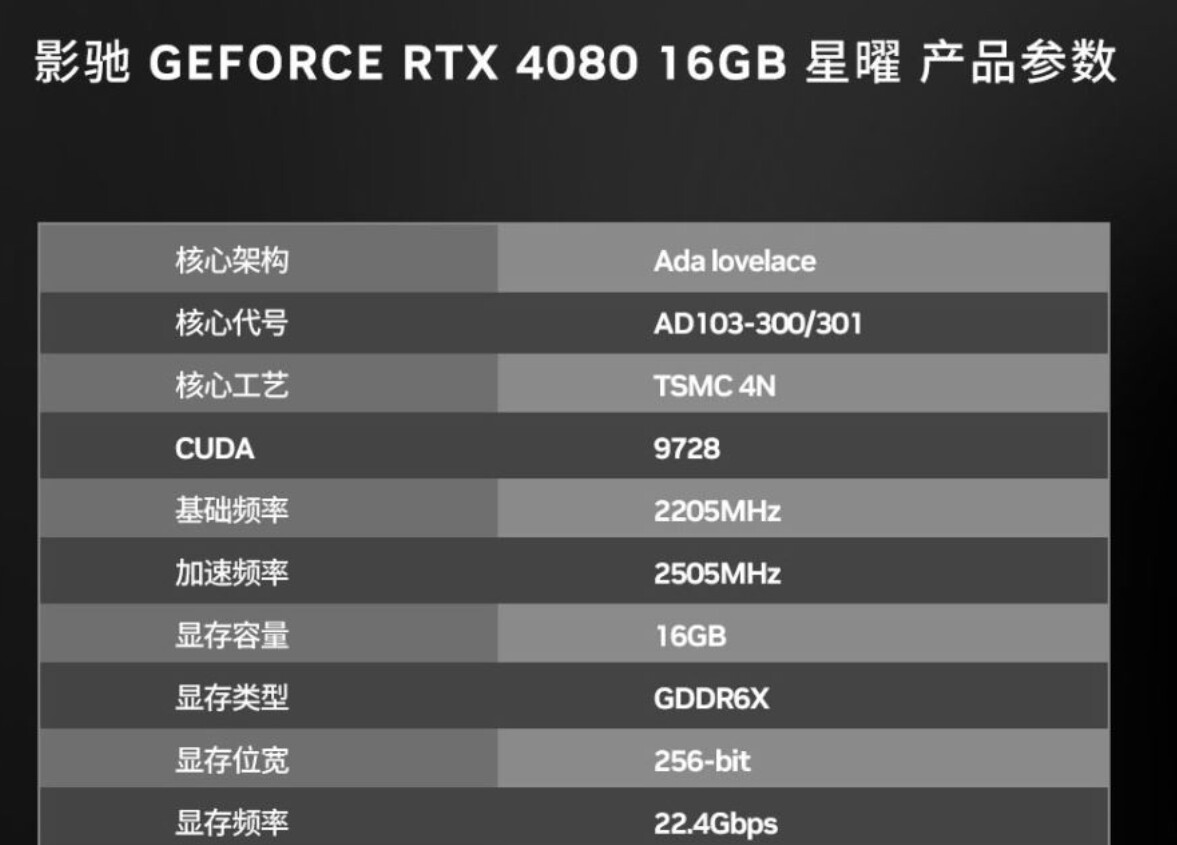
South Korean Company Morumi is Developing a CPU with Infinite Parallel Processing Scaling

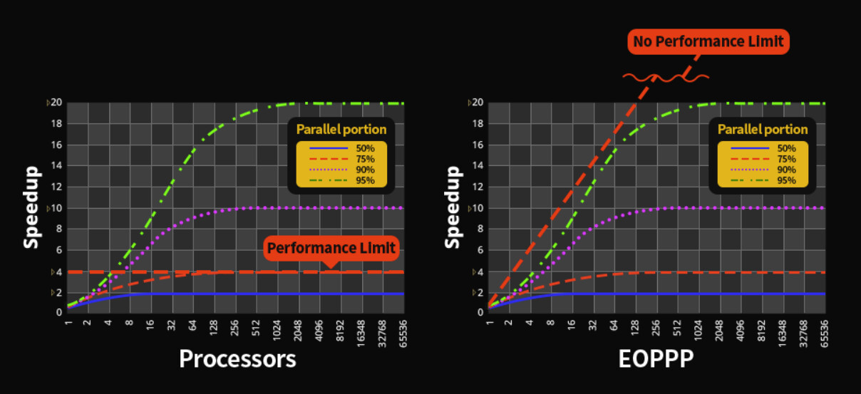
One of the biggest drawbacks of modern CPUs is that adding more cores doesn't equal more performance in a linear fashion. Parallelism in CPUs offer limited scaling for most applications and even none for some. A South Korean company called Morumi is now taking a stab at solving this problem and wants to develop a CPU that can offer more or less infinite processing scaling, as more cores are added. The company has been around since 2018 and focused on various telecommunications chips, but has now started the development on what it calls every one period parallel processor (EOPPP) technology.

EOPPP is said to distribute data to each of the cores in a CPU before the data is being processed, which is said to be done over a type of mesh network inside the CPU. This is said to allow for an almost unlimited amount of instructions to be handled at once, if the CPU has enough cores. Morumi already has an early 32-core prototype running on an FPGA and in certain tasks the company has seen a tenfold performance increase. It should be noted that this requires software specifically compiled for EOPPP and Moumi is set to release version 1.0 of its compiler later this year. It's still early days, but it'll be interesting to see how this technology develops, but if it's successfully developed, there's also a high chance of Morumi being acquired by someone much bigger that wants to integrate the technology into their own products.

Netherlands Government Sets Restrictions on Chip Exports, ASML Responds

Today the Dutch government has published more information on upcoming restrictions on export of semiconductor equipment. These new export controls focus on advanced chip manufacturing technology, including the most advanced deposition and immersion lithography tools. Due to these upcoming regulations, ASML will need to apply for export licenses for shipment of the most advanced immersion DUV systems.

It will take time for these controls to be translated into legislation and take effect. Based on today's announcement, our expectation of the Dutch government's licensing policy, and the current market situation, we do not expect these measures to have a material effect on our financial outlook that we have published for 2023 or for our longer-term scenarios as announced during our Investor Day in November last year.

Axelera AI and Advantech Are Teaming up to Bring the Inference Power of a Data Center to Edge Devices

Axelera AI, the provider of world's most powerful and advanced solutions for AI at the Edge today announces a strategic partnership with Advantech. Combining Advantech's expertise in the embedded and industrial PCs and Axelera AI's disruptive edge AI technology, together they will bring the inference power of a data center to edge devices, enabling customers to process data in real-time, reducing latency while increasing efficiency.

At Embedded World Axelera AI will show its new products, available in a range of industry-standard form factors varying from M.2 modules to vision ready systems. The products combine powerful processing performance with Metis AIPU technology and the easy-to-use Voyager SDK software stack, just at a fraction of the cost and power consumption of today's available solutions.

Hailo Introduces Hailo-15: The First AI-Centric Vision Processors for Next-Generation Intelligent Cameras

Hailo, the pioneering chipmaker of edge artificial intelligence (AI) processors, today announced its groundbreaking new Hailo-15 family of high-performance vision processors, designed for integration directly into intelligent cameras to deliver unprecedented video processing and analytics at the edge. With the launch of Hailo-15, the company is redefining the smart camera category by setting a new standard in computer vision and deep learning video processing, capable of delivering unprecedented AI performance in a wide range of applications for different industries.

With Hailo-15, smart city operators can more quickly detect and respond to incidents; manufacturers can increase productivity and machine uptime; retailers can protect supply chains and improve customer satisfaction; and transportation authorities can recognize everything from lost children, to accidents, to misplaced luggage. "Hailo-15 represents a significant step forward in making AI at the edge more scalable and affordable," stated Orr Danon, CEO of Hailo. "With this launch, we are leveraging our leadership in edge solutions, which are already deployed by hundreds of customers worldwide; the maturity of our AI technology; and our comprehensive software suite, to enable high performance AI in a camera form-factor."

Price War Looming for Mature Fab Nodes in Taiwan

The smaller foundries in Taiwan—at least compared to TSMC—UMC, PSMC and VIS to name the bigger players, but also other less well known foundries that produce chips on mature nodes, are getting ready for what looks like a price war. In all fairness, all of these companies have hiked their prices multiple times over the past couple of years, so it might just be a return to more normal pricing for these nodes that we're looking at. According to UDN media in Taiwan, the smaller foundries are offering discounts that range between 10 and 20 percent for new orders placed with them.

This is largely due to underutilised production lines for some nodes and the companies are trying to increase the utilisation rate of these nodes. The article mentions that the foundries with 8-inch wafer lines are those hardest hit, especially as they've produced more specialised ICs, such as fingerprint sensors, various driver ICs and power management ICs to mention a few. Some of these foundries are now running at 50 to 60 percent of their capacity, which doesn't bode well for the industry. On the other hand, 12-inch fabs aren't nearly as badly hit and might not offer as attractive discounts to potential customers. Another threat to the Taiwanese foundries is Samsung, which is reportedly also offering around a 10 percent discount on its mature nodes.

Ayar Labs Demonstrates Industry's First 4-Tbps Optical Solution, Paving Way for Next-Generation AI and Data Center Designs

Ayar Labs, a leader in the use of silicon photonics for chip-to-chip optical connectivity, today announced public demonstration of the industry's first 4 terabit-per-second (Tbps) bidirectional Wavelength Division Multiplexing (WDM) optical solution at the upcoming Optical Fiber Communication Conference (OFC) in San Diego on March 5-9, 2023. The company achieves this latest milestone as it works with leading high-volume manufacturing and supply partners including GlobalFoundries, Lumentum, Macom, Sivers Photonics and others to deliver the optical interconnects needed for data-intensive applications. Separately, the company was featured in an announcement with partner Quantifi Photonics on a CW-WDM-compliant test platform for its SuperNova light source, also at OFC.

In-package optical I/O uniquely changes the power and performance trajectories of system design by enabling compute, memory and network silicon to communicate with a fraction of the power and dramatically improved performance, latency and reach versus existing electrical I/O solutions. Delivered in a compact, co-packaged CMOS chiplet, optical I/O becomes foundational to next-generation AI, disaggregated data centers, dense 6G telecommunications systems, phased array sensory systems and more.

Biden-Harris Administration Launches First CHIPS for America Funding Opportunity

The Biden-Harris Administration through the U.S. Department of Commerce's National Institute of Standards and Technology today launched the first CHIPS for America funding opportunity for manufacturing incentives to restore U.S. leadership in semiconductor manufacturing, support good-paying jobs across the semiconductor supply chain, and advance U.S. economic and national security.

As part of the bipartisan CHIPS and Science Act, the Department of Commerce is overseeing $50 billion to revitalize the U.S. semiconductor industry, including $39 billion in semiconductor incentives. The first funding opportunity seeks applications for projects to construct, expand, or modernize commercial facilities for the production of leading-edge, current-generation, and mature-node semiconductors. This includes both front-end wafer fabrication and back-end packaging. The Department will also be releasing a funding opportunity for semiconductor materials and equipment facilities in the late spring, and one for research and development facilities in the fall.

Intel Accelerates 5G Leadership with New Products

For more than a decade, Intel and its partners have been on a mission to virtualize the world's networks, from the core to the RAN (radio access network) and out to the edge, moving them from fixed-function hardware onto programmable, software-defined platforms, making networks more agile while driving down their complexity and cost.

Now operators are looking to cross the next chasm in delivering cloud-native functionality for automating, managing and responding to an increasingly diverse mix of data and services, providing organizations with the intelligence needed at the edge of their operations. Today, Intel announced a range of products and solutions driving this transition and broad industry support from leading operators, original equipment manufacturers (OEMs) and independent software vendors (ISVs).

TSMC Said to be Planning Second Fab in Japan

The rumour mill has kicked into high gear this week about TSMC planning a second fab in Japan. The original source is the Nikkan Kogyo newspaper (via Reuters), based in Tokyo, although it's unclear where the actual fab would be located, if it's indeed even happening. According to the paper, the new fab would be focusing on 5 and 10 nanometer chips, but production isn't expected to start until sometime in the second half of this decade. This suggests that these would be mainstream nodes by then, which points to yet another fab for either the vehicle industry or something similar.

The fab is said to cost more than a trillion yen, or over US$7.4 billion to build. TSMC's CEO C.C. Wei was asked about the potential fab during TSMC's latest earnings call, but simply said that the company had nothing further to add. TSMC is of course busy building a fab in Japan on Kyushu island, but as it'll have a node capacity for 12 to 16 nm parts, it makes sense that TSMC would already be planning for an extension of said fab that can produce on more advanced nodes as its customers will be moving to more advanced nodes over time.

AMD Expected to Occupy Over 20% of Server CPU Market and Arm 8% in 2023

AMD and Arm have been gaining up on Intel in the server CPU market in the past few years, and the margins of the share that AMD had won over were especially large in 2022 as datacenter operators and server brands began finding that solutions from the number-2 maker growing superior to those of the long-time leader, according to Frank Kung, DIGITIMES Research analyst focusing primarily on the server industry, who anticipates that AMD's share will well stand above 20% in 2023, while Arm will get 8%.

Prices are one of the three major drivers that resulted in datacenter operators and server brands switching to AMD. Comparing server CPUs from AMD and Intel with similar numbers of cores, clockspeed, and hardware specifications, the price tags of most of the former's products are at least 30% cheaper than the latter's, and the differences could go as high as over 40%, Kung said.

Intel Xeon W-3400/2400 "Sapphire Rapids" Processors Run First Benchmarks

Thanks to the attribution of Puget Systems, we have a preview of Intel's latest Xeon W-3400 and Xeon W-2400 workstation processors based on Sapphire Rapids core technology. Delivering up to 56 cores and 112 threads, these CPUs are paired with up to eight TeraBytes of eight-channel DDR5-4800 memory. For expansion, they offer up to 112 PCIe 5.0 lanes come with up to 350 Watt TDP; some models are unlocked for overclocking. This interesting HEDT family for workstation usage comes at a premium with an MSRP of $5,889 for the top-end SKU, and motherboard prices are also on the pricey side. However, all of this should come as no surprise given the expected performance professionals expect from these chips. Puget Systems has published test results that include: Photoshop, After Effects, Premiere Pro, DaVinci Resolve, Unreal Engine, Cinebench R23.2, Blender, and V-Ray. Note that Puget Systems said that: "While this post has been an interesting preview of the new Xeon processors, there is still a TON of testing we want to do. The optimizations Intel is working on is of course at the top, but there are several other topics we are highly interested in." So we expect better numbers in the future.
Below, you can see the comparison with AMD's competing Threadripper Pro HEDT SKUs, along with power usage using different Windows OS power profiles:

Marvell and AWS Collaborate to Enable Cloud-First Silicon Design

Marvell Technology, Inc., a leader in data infrastructure semiconductor solutions, announced today that it has selected Amazon Web Services, Inc. (AWS) as its cloud provider for electronic design automation (EDA). A cloud-first approach helps Marvell to rapidly and securely scale its service on the world's leading cloud, rise to the challenges brought by increasingly complex chip design processes, and deliver continuous innovation for the expanding needs across the automotive, carrier, data center, and enterprise infrastructure markets it serves. The work extends the longstanding relationship between the two companies—Marvell is also a key semiconductor supplier for AWS, helping the company support the design and rapid delivery of cloud services that best meet customers' demanding requirements.

EDA refers to the specialized and compute-intensive processes used in chip making and is a critical piece of Marvell's R&D. Over the years, the number of transistors on an integrated chip has increased exponentially. Each advance in chip design calls for a calculated application of software modules overseeing logic design, debugging, component placement, wire routing, optimization of time and power consumption, and verification. Due to the computationally intensive nature of EDA workloads, it is no longer cost-effective or timely to run EDA on premises. By powering its EDA with AWS, Marvell leverages an unmatched portfolio of services including secure, elastic, high-performance compute capacity in the cloud to solve challenges around speed, latency, security of IP, and data transfer.

GlobalFoundries Reports Fourth Quarter and Fiscal Year 2022 Financial Results

GlobalFoundries Inc. (GF) (Nasdaq: GFS) today announced preliminary financial results for the fourth quarter and fiscal year ended December 31, 2022.

Key Fourth Quarter Financial Highlights
Revenue of $2,101 million, up 14% year-over-year.
Gross margin of 29.6% and adjusted gross margin of 30.1%.
Net income of $668 million.
Adjusted EBITDA of $821 million.
Cash, cash equivalents and marketable securities of $3,346 million.

Winbond Joins UCIe Consortium to Support High-performance Chiplet Interface Standardisation

Winbond has joined the UCIe (Universal Chiplet Interconnect Express) Consortium, the industry Consortium dedicated to advancing UCIe technology. This open industry standard defines interconnect between chiplets within a package, enabling an open chiplet ecosystem and facilitating the development of advanced 2.5D/3D devices.

A leader in high-performance memory ICs, Winbond is an established supplier of known good die (KGD) needed to assure end-of-line yield in 2.5D/3D assembly. 2.5D/3D multichip devices are needed to realize the exponential improvements in performance, power efficiency, and miniaturization, demanded by the explosion of technologies such as 5G, Automotive, and Artificial Intelligence (AI).

Intel Asking Germany for More Money, Set to Potentially Invest in Vietnam

To date, Intel has been promised almost €6.8 billion in subsidies from the federal German government, but apparently this isn't enough for Intel, as the company is now asking for an additional €3.2 billion, for a total of €10 billion is subsidies for its Magdeburg fab. The total investment in the fab in Magdeburg—which was announced back in March 2022—is said to be around €33 billion. In other words, Intel is asking Germany to pitch in almost a third of the cost for its shiny new fab. According to an Intel spokesperson quoted by the Register, Intel is worried about the current geopolitical situation and that the demand for semiconductors has declined, plus the fact that inflation has made everything much more expensive. Intel's Arizona fabs ended up costing an extra US$5 billion, which is about a third extra compared to the original cost estimate, so it's not hard to see why Intel is asking for more money here.

At the same time, the Vietnamese government jumped the gun and announced that Intel is looking at investing US$3.3 billion in the country, as part of an announcement of investments of a total of US$7.4 billion in Ho Chi Minh, by foreign companies. The additional US$4.1 billion investments apparently hinges on Intel's investment in the country, more specifically in the Saigon Hi-Tech Park. The official stance from Intel is that "Vietnam is an important part of our global manufacturing network, but we have not announced any new investments." It's unclear what the exact plans are, but Intel is said to have met up with government officials in Vietnam, according to Bloomberg. It's likely that it would be some kind of chip packaging facility, much like what Intel and AMD already has in Malaysia and China, among other places.

Samsung Electronics Announces Fourth Quarter and FY 2022 Results, Profits at an 8-year Low

Samsung Electronics today reported financial results for the fourth quarter and the fiscal year 2022. The Company posted KRW 70.46 trillion in consolidated revenue and KRW 4.31 trillion in operating profit in the quarter ended December 31, 2022. For the full year, it reported 302.23 trillion in annual revenue, a record high and KRW 43.38 trillion in operating profit.

The business environment deteriorated significantly in the fourth quarter due to weak demand amid a global economic slowdown. Earnings at the Memory Business decreased sharply as prices fell and customers continued to adjust inventory. The System LSI Business also saw a decline in earnings as sales of key products were weighed down by inventory adjustments in the industry. The Foundry Business posted a new record for quarterly revenue while profit increased year-on-year on the back of advanced node capacity expansion as well as customer base and application area diversification.

Qualcomm Allegedly Preparing a Rival to Apple M SoC, Codenamed Hamoa

Qualcomm has been working on its Snapdragon SoCs for quite some time now, with massive success in the mobile phone space. However, the company's processors needed to be up to the task regarding laptops. For a user to not look at x86 offerings, the only remaining performant alternatives are Apple's M processors. In 2021 Qualcomm purchased the Nuvia team that was developing massively efficient and high-performance IP for laptops, similar to Apple M processors. Today, according to the insights from Kuba Wojciechowski (@Za_Raczke) on Twitter, we have some potential information about the upcoming Nuvia-powered SoC codenamed Hamoa.

According to the Twitter thread, Qualcomm's Hamoa processors are part of the Snapdragon 8xc Gen 4 compute platform and feature up to eight high-performance P-cores and four low-power E-cores, all based on Nuvia's IP. Allegedly the P-cores are being tested at 3.4 GHz, while the E-cores are tested at 2.5 GHz. The SoC splits CPU cores into blocks, each being a four-core group with 12 MB of shared L2 cache. There is also an 8 MB L3 cache structure; it needs to be clarified whether it is per core block or for the entire SoC. The chip employs 12 MB of system-level cache, with 4 MB of memory for graphics-related tasks handled by iGPU. The iGPU of choice is Adreno 740, with all modern APIs supported. Discrete graphics solutions are supported by the top-end SKUs, which allow eight PCIe 4.0 lanes to be directed toward dGPU, along with an additional four PCIe 4.0 lanes for NVMe SSD. For RAM, the chip uses up to 64 GBs of LPDDR5X eight-channel memory with up to 4.2 GHz speeds. Chip's media engines are structured to support decoding up to 4K120 and encode up to 4K60 with AV1.

NVIDIA Updates GeForce RTX 4080 Silicon with AD103-301 SKU

NVIDIA has reportedly begun shipping NVIDIA GeForce RTX 4080 graphics cards with a newer GPU SKU that changes the requirement for PCB design and is set to lower manufacturing costs. Previously, the company shipped its AD103-300-A1 SKU to power the GeForce RTX 4080 graphics cards. However, the new AD103-301 SKU will power the upcoming RTX 4080 cards that the company plans to ship to its AIBs and possibly use in the reference design. With the new 301 version, the GPU performance and power envelope should not change. What does change is the PCB design requirements, as the new SKU revision possesses a different chip pinout that doesn't correspond to the old design.

HKEPC has reported that GPUs with AD103-301 SKU are shipping, while VideoCardz confirms the AIB update with Gainward also offering updated cards. GALAX offers RTX 4080 models with either AD103-300/301 as well. Additionally, the GeForce RTX 4070 Ti will also see an SKU update, with AD104-250 being replaced by AD104-251. With these new silicon revisions, customers will not see any difference. However, the AIBs and NVIDIA could see a cost reduction to improve margins. HKEPC estimates around $1 BOM cost reduction with the new SKU, which will make a difference in thousands of cards shipped.

Tachyum Closes DDR5 Timing at over 6400MT/s Providing Massive Bandwidth for Prodigy Chip

Tachyum today announced that the IP components -DDR5 RAM controller and high-performance, low-power DSP-based PHY - incorporated into the Prodigy Universal Processor have allowed it to achieve speeds of 6400 MT/s at nominal voltage for Prodigy chip which provides headroom for expected speeds of up to, or even over, 7200 MT/s.

The critical components supplied by a global leader in high-speed DDR DRAM controllers and DDR DRAM PHYs for the world's technology infrastructure, have enabled Tachyum engineers to integrate its IP into Prodigy less than 7 months after entering into a technology partnership. The quality of this IP and the support provided by working closely with Tachyum engineers have allowed the company to close DDR5 timings in record time.

Montage Technology PCIe 5.0/CXL 2.0 Retimer Chip Achieves Mass Production

Montage Technology, a leading data processing and interconnect IC design company, announced today that its PCIe 5.0/CXL 2.0 Retimer has successfully achieved mass production. This chip is a key upgrade based on Montage's PCIe 4.0 Retimer, providing a stable and reliable PCIe 5.0 and CXL 2.0 interconnect solution with high bandwidth and low latency for the cloud and high-performance computing market.

Montage's PCIe 5.0/CXL 2.0 Retimer employs advanced signal conditioning technologies to improve signal integrity and increase the effective transmission distance of high-speed signals. Compliant with relevant PCI-SIG and CXL specifications, the chip meets mainstream package requirements, supports transfer rate up to 32 GT/s, and takes the lead in supporting ultra-low transmission latency of less than 5 ns. The chip supports various complex system topologies such as SRIS and Retimer cascading, offering an ideal solution to address the PCIe/CXL signal integrity challenges in next-generation servers, enterprise storage, and AI acceleration systems. The PCIe 5.0/CXL 2.0 Retimer has passed extensive interoperability testing with a variety of compute, storage and networking products, such as CPU, PCIe switches, SSDs, GPUs and NICs, thus laying a solid foundation for the large-scale deployment of cloud computing and data centers.

Powercast Wants to Put a RF Power Transmitter into Every Room in Every House

Powercast Corporation, the leader in radio-frequency (RF)-based over-the-air wireless power technology, has unveiled its Ubiquity transmitter, an ultra-low-cost RF power transmitter which was selected as a CES 2023 Innovation Award Honoree in three categories: Smart Home, Embedded Technologies and Sustainability, Eco-Design & Smart Energy.

Designed to be the industry's most economical RF wireless transmitter, Powercast has lowered the barrier to entry where RF wireless power can actually become ubiquitous with multiple RF transmitters covering every home. Ubiquity will be on display in Powercast's booth #52311 at the Venetian Expo in the Smart Home Marketplace during CES 2023 in Las Vegas, January 5 - 8, 2023.

MediaTek Introduces Global Ecosystem of Consumer-Ready Wi-Fi 7 Products at CES 2023

MediaTek, one of the first adopters of Wi-Fi 7 technology, will be demonstrating a full ecosystem of production-ready devices featuring the next generation of wireless connectivity for the first time at CES 2023. These products are the culmination of MediaTek's investment in Wi-Fi 7 technology, focusing on reliable and always-on connected experiences on a wide variety of devices in several product categories, including residential gateways, mesh routers, televisions, streaming devices, smartphones, tablets, laptops, and more.

As the most current and powerful Wi-Fi standard, Wi-Fi 7 utilizes record-breaking 320 MHz channel bandwidth and 4096-QAM modulation to greatly improve overall user experience. Multi-Link Operation (MLO) also enables the Wi-Fi connection to aggregate channel speeds and alleviate link interruption in congested environment for time-demanding applications.

South Korean Chip Makers Affected by Slump in Chip Demand

It's not just TSMC and the other Taiwanese chip makers that are seeing a dip in demand, the Korean chip makers have seen a slump of 15 percent in the past four months, compared to 2021. This is said to be the biggest drop in chip demand since 2009 according to data from Statistics Korea. There's a combination of factors behind the slump in demand, especially when it comes to memory related products, where inventories already are high, combined with inflation and a low demand.

According to the Financial Times, an analyst at JPMorgan in Korea isn't expecting things to improve until 2024 at the earliest. Just like Micron and Kioxia, SK hynix is looking at cutting spending on new fabs and production lines, although as TPU reported earlier this week, Samsung is going its own way, by continuing to invest in new fabs and production lines. Samsung is expected to have a capex of US$37.5 billion this year back in October, although based on the increase in costs, the capex would have increased in the fourth quarter of the year. On the plus side, it seems like the shortage of semiconductors should ease in 2023 and hopefully return to more normal levels.

TSMC to Mark 3 nm Mass Production Start, Looking at Potential New Fabs in Japan and Germany

According to news out of Taiwan, TSMC will hold a ceremony to mark the official mass production start of its 3 nm node on the 29th of December. This is said to help "shatter doubts about de-Taiwanization" or in simpler terms, that Taiwan will lose its golden goose as TSMC invests abroad. The 3 nm fab—known as fab 18—is based in southern Taiwan's Tainan and the ceremony also marks the start of an expansion of TSMC's most advanced fab. TSMC is said to be kicking off its N3E node production sometime in the second half of 2023, followed by its N3P node in 2024, all of which should take place at fab 18, which also produces 5 nm wafers.

In related news, according to Reuters, a Japanese lawmaker from the ruling party has said that TSMC is considering a second plant in Japan, in addition to its current joint venture that is already under construction. TSMC's response to Reuters was that the company isn't ruling out Japan for future fabs, but that the company doesn't have any current plans. At the same time, TSMC is said to be sending executives to Dresden, Germany in early 2023, for a second round of talks about building a fab to help support the European auto industry, although this would be a 28/22 nm fab, which is far from cutting edge these days, although a lot more advanced than most fabs making chips for the auto industry.

Intel Reorganises its Graphics Chip Division, Raja Koduri Seemingly Demoted

Big things are afoot at Intel's graphics chip division once again, as the company has just broken up its Accelerated Computing Systems and Graphics (AXG) business unit which will result in some big changes. For starters, Raja Koduri has been—what we can only refer to as—demoted, given he's back to being chief architect rather than being in charge of the AXG business unit. Some of his staff will be moved to other business units inside Intel as the AXG business unit will cease to exist. This doesn't mean Intel will stop making discrete consumer GPUs, with at least the Battlemage/Arc B-series launch still being planned to take place sometime in 2023.

At the same time, it looks like Raja Koduri will be out of action for what is likely to be at least a month since he posted on Twitter that he's had emergency back surgery while on a business trip. How this will affect his transition back to his role as chief architect is anyone's guess at this point in time. However, he will not be focusing solely on GPUs in the future, but the broader range of products that Intel offers—particularly the integration of GPU, CPU and AI architectures at Intel. We've posted an official statement from Intel after the break, which Intel provided to Tom's Hardware. We also wish Raja a speedy recovery!
Return to Keyword Browsing
May 8th, 2024 12:51 EDT change timezone

New Forum Posts

Popular Reviews

Controversial News Posts