News Posts matching #nForce 200

Return to Keyword Browsing

Gigabyte Responds to MSI's Bluff Call

A little earlier this month, MSI's PR team dished out a presentation in which they claimed that Gigabyte was misleading buyers into thinking that as many as 40 of its recently-launched motherboards were "Ready for Native PCIe Gen.3". MSI tried to make its argument plausible by explaining what exactly goes into making a Gen 3-ready motherboard. The presentation caused quite some drama in the comments. Gigabyte responded with a presentation of its own, in which it counter-claimed that those making the accusations ignored some key details. Details such as "what if the Ivy Bridge CPU is wired to the first PCIe slot (lane switches won't matter)?"

EVGA Rolls Out Trio of Z68 Motherboards

After much delay, EVGA released its first wave of LGA1155 motherboards based on the Intel Z68 chipset featuring Intel Smart Response technology. Quite surprisingly, none of EVGA's Z68 motherboards feature display outputs. The series is topped by Z68 FTW, designed for enthusiasts and overclockers; followed by Z68 SLI, geared for gamers with NVIDIA SLI graphics setups; and Z68 SLI Micro, an SLI-ready board in the micro-ATX form-factor.

The Z68 FTW uses a similar layout to the P67 FTW. It uses a strong VRM to power the CPU and memory, it provides as many as six PCI-Express x16 slots, making use of a nForce 200 bridge chip that makes it 3-way and 4-way SLI ready. It is loaded with overclocker-friendly features such as EVbot support, a front-panel OC controller, and an overclocking gauge. The Z68 FTW is also available as a package without those two accessories.

ZOTAC Unveils Z68ATX-A-E Fully Loaded LGA1155 Motherboard

ZOTAC showed off its new, upcoming socket LGA1155 motherboard based on the Intel Z68 chipset, the Z68ATX-A-E. This is a full-blown ATX form-factor motherboard, that throws in plenty of connectivity. The LGA1155 socket is powered by a 20-phase VRM, that makes use of super-ML capacitors to condition power. The board uses an nForce 200 bridge chip that occupies the PCI-E x16 link of the processor, giving out PCI-Express 2.0 x16 links, further split between four PCI-Express 2.0 x16 slots. A PLX-made PCI-E 1.1 x4 to 3 PCI-E 2.0 x1 bridge chip is also present, driving additional controllers such as three of the four USB 3.0 controllers giving out 8 ports (four by headers). The board is designed to support 3-way and 4-way SLI.

Display connectivity includes two DVI, with the possibility of a DVI-HDMI dongle being bundled, other connectivity includes 8-channel HD audio, WiFi b/g/n, and dual gigabit Ethernet. In the storage department there appear to be four SATA 6 Gb/s, four SATA 3 Gb/s. There is a suite of overclocker-friendly features, including triple-redundant BIOS, voltage measurement points, and diagnostic LED display. The ZOTAC logo in the heatsink over the NF200 lights up. While the placard speaks of Intel 311 SSD, we're not sure if they're talking about an mSATA fixed SSD, we can't see one. Perhaps a 2.5-inch SATA 311 Series SSD comes bundled.

ASUS Readies Z68-based ROG Maximus IV Extreme-Z Motherboard

When Intel's Sandy Bridge platform was launched, P67 Express was perceived as the top of the line discrete graphics chipset that gives performance segment users everything they'll ever need. ASUS hence based its prestigious ROG Maximus branded motherboard based on it, and came up with the Maximus IV series. With Intel releasing a higher-end chipset with the Z68 Express, ASUS decided to redo its socket LGA1155 ROG motherboard lineup, with the Maximus IV Extreme-Z. The new motherboard gives users access to the processors' embedded graphics via a HDMI port, and gives them the benefit of Intel Smart Response technology that P67 lacks.

The Maximus IV Extreme-Z looks similar to its P67-based cousin. Based on the Intel Z68 chipset, the motherboard uses an NVIDIA nForce 200 bridge chip to ensure PCI-Express connectivity to up to four graphics cards, supporting NVIDIA SLI and AMD CrossFireX. The CPU is powered by ASUS Digi+ Extreme VRM, backed by high-grade components and proadlizers to condition power. There are four DIMM slots supporting dual-channel DDR3-2000 MHz memory by overclocking. Expansion slots include four PCI-Express 2.0 x16 (x16/NC/x16/NC or x8/x8/x8/x8), there's also a PCI-E x1 and open-ended PCI-E x4.

Gigabyte Z68X-UD7 Spotted in Taiwan Stores

Stores in Taiwan have started stocking up on Gigabyte's latest high-end LGA1155 motherboard, the GA-Z68X-UD7 B3. Based on the new Z68 chipset that combines the overclocking capabilities of P67 with the Flexible Display Interface (FDI) feature of H67, Z68 will be Intel's most functional desktop chipset for the LGA1155. Gigabyte's board carries forward the feature-set of the P67A-UD7, and adds a GUI-based Hybrid EFI setup program. Quite surprisingly, there are no display outputs, so we're not quite sure why the designers opted for Z68 in the first place.

The GA-Z68X-UD7 uses a 24-phase VRM that uses driver-MOSFETs to power the CPU, four DDR3 DIMM slots to support dual-channel memory, four PCI-Express x16 slots supporting 3-way SLI and CrossFireX. Gigabyte is probably using an NVIDIA nForce 200 bridge chip for the additional PCI-E lanes. Storage connectivity includes four SATA 6 Gb/s, six SATA 3 Gb/s, and two eSATA/USB combo ports. There are at least four USB 3.0 ports. Gigabyte's new board will reach western markets later this month, after Z68's formal launch.

EVGA Readies P67 FTW B3 LGA1155 Motherboard

After quite some lull, a new motherboard by EVGA is taking shape, the EVGA P67 FTW B3. As the name suggests, it is a top-tier motherboard by the company, based on the Intel P67 B3 chipset. The P67 FTW ("for the win", in gamer jargon) supports LGA1155 Intel Core i3/i5/i7 processors, and is geared for extreme overclocking of CPU and GPUs, and is particularly laid out for supporting 3-way and 4-way NVIDIA SLI. The board uses an NVIDIA nForce 200 bridge chip over the processor's PCI-Express 2.0 x16 link to give out two x16 links, which are further configured as four x8 links, if four x16 slots are populated with graphics cards. The board uses a 12-phase CPU VRM with split heatsinks, the CPU is wired to four DDR3 DIMM slots, supporting dual-channel DDR3.

Storage connectivity includes two internal SATA 6 Gb/s, four SATA 3 Gb/s; other connectivity includes 8-channel HD audio, two gigabit Ethernet interfaces, USB 3.0, and a number of USB 2.0. There are several overclocker-friendly features, such as support for EVGA EVBot, an external overclock control and monitoring module, jumpers to toggle specific PCI-Express slots, consolidated voltage measurement points, onboard power/reset buttons, and LED POST diagnostic readout. A strong VRM and feature-rich BIOS should top it up. The new board is priced at a juicy US $200, and should be available soon.

NVIDIA SLI on AMD Chipset Motherboards Soon

NVIDIA SLI multi-GPU technology is going through a rough patch on the AMD platform, with very few NVIDIA nForce 900 series motherboards available/sold. With AMD looking to come back strong in the performance CPU market (which might cause high-end gaming PC users to switch platforms), it is wise on the part of NVIDIA to make SLI available to AMD platform users in some form. NVIDIA is making a cautious move: licensing SLI to motherboard vendors in the same protocol in which it licenses them to provide NVIDIA SLI support on Intel 5-series and 6-series chipset based motherboards.

This move is particularly wise because NVIDIA wouldn't need to invest on making a chipset (though it can) for AMD's upcoming "Bulldozer" CPUs, and still get licensing fees for NVIDIA SLI. That way, it wouldn't have to rely on the platform's overall market success. NVIDIA will offer SLI licenses to motherboards based on AMD's upcoming 9-series chipset, particularly to models that lack integrated Radeon graphics (that's AMD 990FX, and AMD 990X). It will offer 2-way SLI licenses to motherboards running AMD 990X, and 3-way/2-way licenses to boards based on AMD 990FX. It won't offer nForce 200 bridge chips. Further, only those motherboard manufacturers that are currently tied up with NVIDIA for SLI licenses on Intel platform, will be granted SLI licenses on AMD platform.

Galaxy Designs its Own Dual GeForce GTX 460 Graphics Card

After EVGA's release of its GeForce GTX 460 2WIN dual-GPU graphics card earlier this week, Galaxy wasn't going to sit back. The company rushed in with pictures of its own dual-GeForce GTX 460 graphics card. The card is still in the works, and Galaxy was only able to display its PCB. Galaxy chose a milky-white PCB, which uses two GF104 cores in an internal SLI, powered by a strong VRM circuitry. Each GPU has 336 CUDA cores, and is wired to 1 GB of GDDR5 memory over a 256-bit wide memory interface.

Further, both display outputs of each GPU is wired out in the form of DVI connectors, making the card a single-piece 3D Vision Surround solution. Interestingly, Galaxy chose a bridge chip other than nForce 200 to run the SLI on a stick solution. If Galaxy's implementation clicks, then every AIC partner with its own R&D could work on their own dual-GPU cards, currently, they're held back by non-supply of nForce 200.

NVIDIA GeForce GTX 590 Launch Date is March 22

The dust seems to have settled down, after AMD's launch of the Radeon HD 6990, extending the red-team's performance lead previously held precariously by the Radeon HD 5970, to the GeForce GTX 580. It looks like NVIDIA will challenge the performance leadership with GeForce GTX 590, a dual-GPU graphics card that uses two GF110 GPUs (the ones on GTX 570 and GTX 580), for an SLI-on-a-stick solution. Rumors of NVIDIA working on this card became concrete as early as in November 2010, when NVIDIA's reference board became public for the first time.

Latest reports suggest that NVIDIA has chosen March 22 as the launch day of GeForce GTX 590. Incidentally, that is also the launch date of EA/Crytek's much-hyped, initially DirectX 9 action/shooter game, Crysis 2. GeForce GTX 590 uses two GF110, though the shader configuration and clock speeds are not known. Since NVIDIA is chasing the top-spot, you can expect the most optimal configuration for the GF110s. A total of 3 GB (1536 MB per GPU system) on board, and NVIDIA's workhorse PCI-E bridge, nForce 200 will be the traffic cop and radio station between the two GPUs. The card will be able to do 3DVision Surround (NVIDIA's multi-display single head technology comparable to ATI Eyefinity) on its own, without needing a second card.

EVGA P67 Classified Motherboard Looks Ferocious

EVGA unveiled its next enthusiast-grade motherboard, the P67 Classified. The board is designed for upcoming "Sandy Bridge" processors from Intel in the LGA1155 package, and uses the Intel P67 Express chipset. EVGA's main design goes seem to be: 1. giving the processor a strong VRM that helps with overclocking; and 2. to expand the board's PCI-Express resources using an nForce 200 bridge chip. The CPU is powered by a 12-phase VRM that draws power from two 8-pin EPS connectors. Knowing EVGA, the CPU socket is of premium-grade, with higher gold content on the pins. The four DDR3 DIMM slots are powered by a 3-phase VRM. The main ATX power connector is angled for better aesthetics.

Expansion slots include six PCI-Express 2.0 x16 (electrical x16/x8;x1;x16/x8;x8;x16/x8;x8), making the board capable for 4-way SLI. A single PCI-E x1 is tucked away on top. Connectivity includes two internal SATA 6 Gb/s, four internal SATA 3 Gb/s, two front-panel and two rear-panel USB 3.0, 8-channel HD audio, two gigabit Ethernet controllers, FireWire, and eSATA. The board supports a plethora of overclocker-friendly technologies, including EVGA's EV-Bot module. One can expect more information once Intel's upcoming processors are out.

ASUS P8P67 WS Revolution Motherboard Pictured

ASUS unveiled its new workstation-grade socket LGA1155 motherboard that supports 2011-series Core i3/5/i7 processors, as well as, upcoming Xeon LGA1155 processors, the P8P67 WS Revolution. It is packed to the brim with features. To begin with, the CPU is powered by a 16+2 phase digital VRM, the socket is wired to four DDR3 DIMM slots for dual-channel memory, supporting speeds of over DDR3-2200 MHz. There are four PCI-Express 2.0 x16 slots, supporting 3-way SLI/CrossFireX, probably using a bridge chip such as the NVIDIA nForce 200, and three PCI-E x1.

Storage features include four SATA 6 Gb/s ports, and four SATA 3 Gb/s. Connectivity features include two Intel GbE controllers, 8+2 channel HD audio, two USB 3.0 ports, and a number of USB 2.0 ports. Other features include a system diagnostics card, EPU energy-efficiency processor, TurboV Processing Unit (TPU), and Quick Gate instant-on OS. ASUS will announce pricing when it most probably releases this board in January.

Zotac Designs GeForce GTX 460 X2 Graphics Card

Zotac is another NVIDIA partner who isn't pleased that the GeForce GTX 480 isn't holding performance leadership, but has the engineering potential to outdo it. Earlier in June, Galaxy showed off a dual Fermi graphics card that makes use of two GF100 graphics processors in the GeForce GTX 465 configuration. Zotac waited for a more mature implementation of the Fermi architecture, found out that the GF104-based GeForce GTX 460 isn't lacking much in performance compared to the GTX 465, with vastly better thermal specifications, and went on to design its latest high-end card, which it now refers to as the Zotac GeForce GTX 460 X2. The card makes use of two GeForce GTX 460 1 GB GPUs in an internal SLI, much like every other dual-GPU NVIDIA card.

The card uses an NVIDIA nForce 200 bridge chip to semaphore and broadcast data between the two GPUs, a dual 3+1+1 phase VRM that draws power from two 8-pin PCI-E power connectors, and display connectivity is relayed to the rear-panel from both the GPUs, that's four dual-link DVI, and one mini-HDMI. What this also means is that with just this one card, you can use the 3D Vision Surround feature, while retaining SLI multi-GPU scaling. If that's not all, there's a SLI connector, which lets you pair this with another card of its kind, for GTX 460 Quad-SLI. Zotac is yet to finalize a cooling solution to suit it best. GF104 could be NVIDIA's easiest route to a dual-GPU graphics card that establishes performance leadership. The GF104 physically has 384 CUDA cores (336 on Zotac's card, since it's in the GTX 460 configuration), and has shown to be capable of high GPU/Shader clock speeds. More details about Zotac's card are awaited.

EVGA Intros X58 Classified3 Motherboard

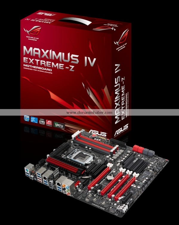
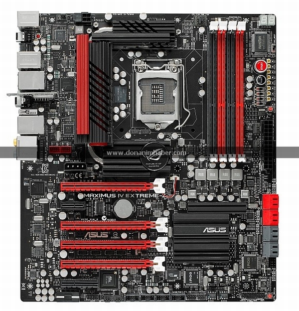
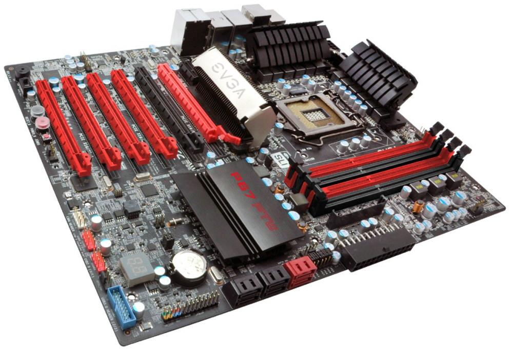
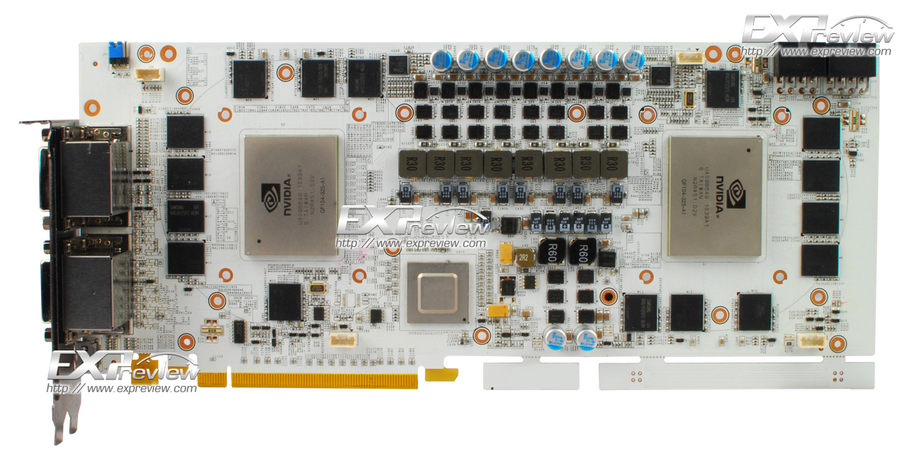
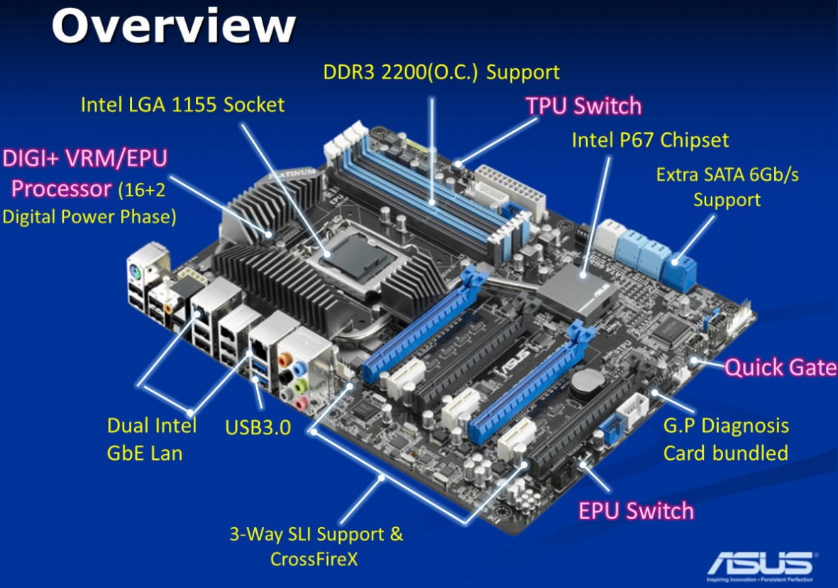
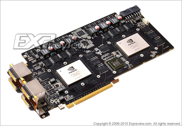
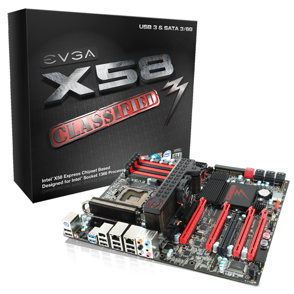
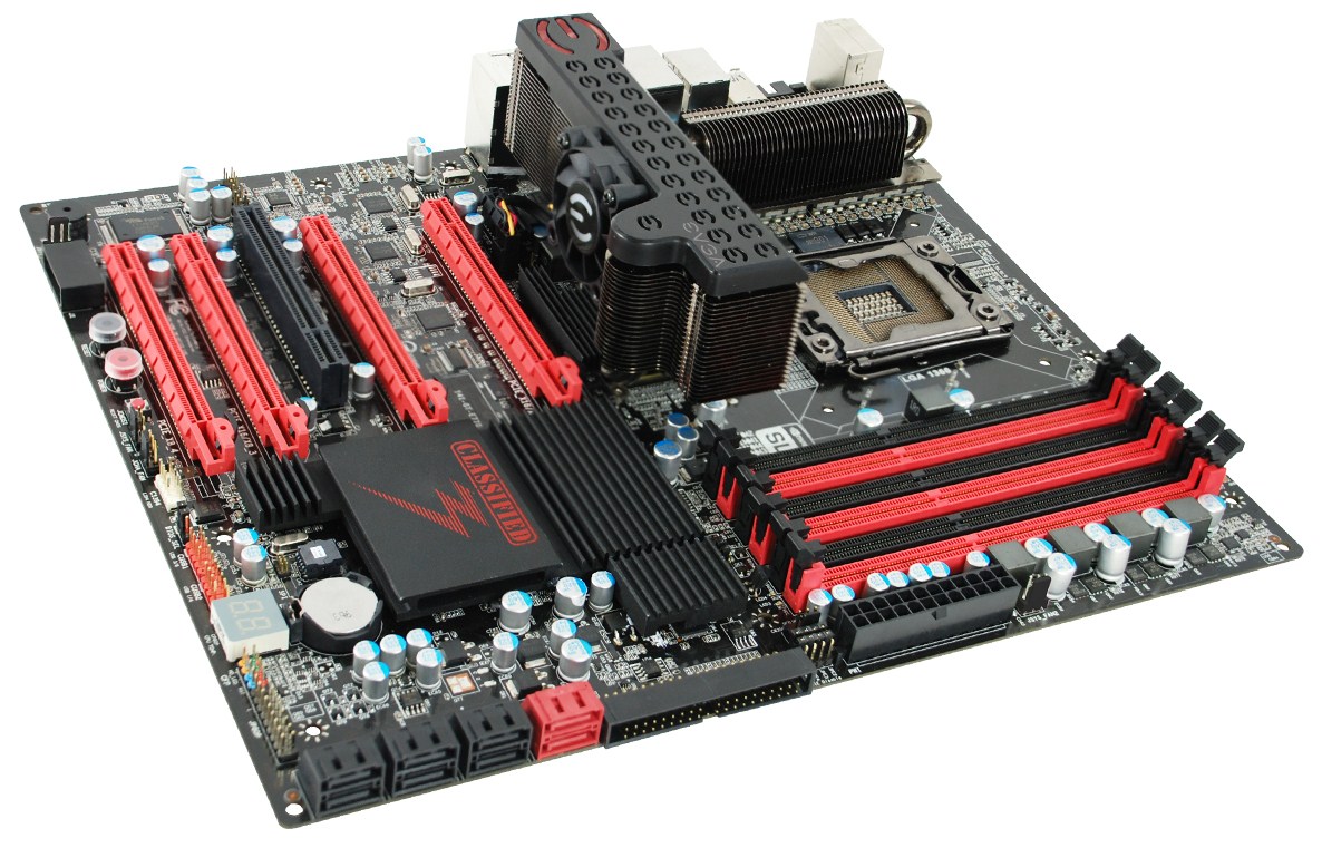
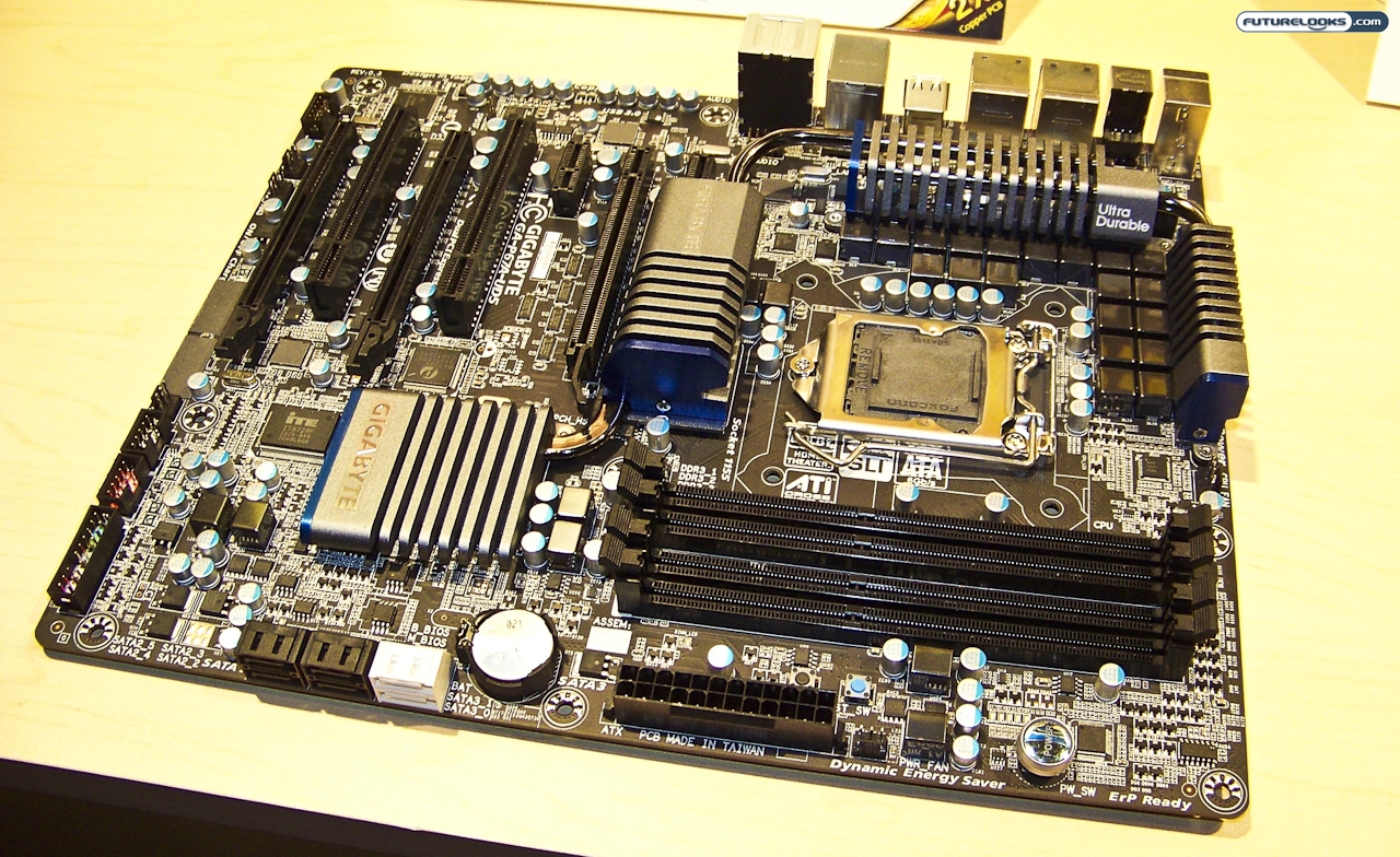
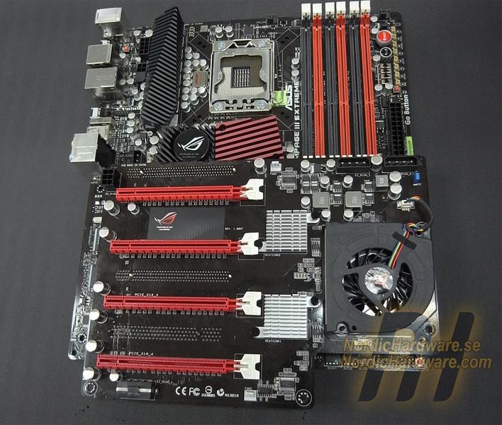
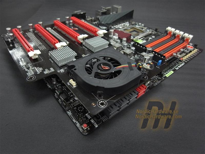
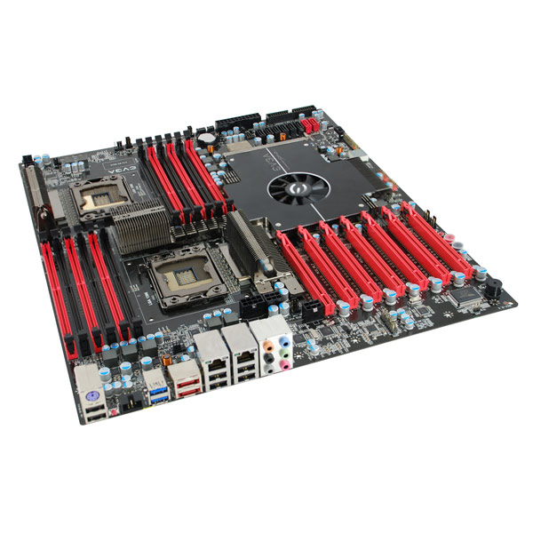
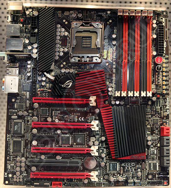
EVGA introduced the third motherboard in its socket LGA1366 lineup refresh, the X58 Classified3 (model number 141-GT-E770-A1). EVGA's motherboard lineup refresh, usually denoted by a "3" suffix to the model name, is centered on feature additions that include USB 3.0, SATA 6 Gb/s, and out of the box support for the latest processors. The X58 Classified3 sports a high-end 10-phase digital PWM voltage regulation for the CPU that makes use of a Prodalizer for better power conditioning. Unlike the original X58 Classified design and like the X58 Classified E760, this board does not make use of any additional nForce 200 bridge chips, the four PCI-Express 2.0 x16 slots are wired directly to the X58 northbridge (configured as x16, NC, x16, NC; or x16, NC, x8, x8; or x8, x8, x8, x8; depending on how they're populated). The PWM area is cooled by its own heatsink, while that over the X58 northbridge is elaborate, complete with a fan. The ICH10R southbridge has a large heatsink to chill with. Other expansion slots include one each of PCI-E x1 and PCI.

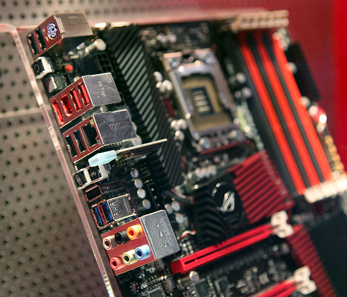
Connectivity features include two SATA 6 Gb/s internal ports (color coded red), six internal SATA 3 Gb/s ports, and one legacy IDE connector, two USB 3.0 ports (rear), a number of USB 2.0 ports, 8-channel HD audio, dual gigabit Ethernet, and FireWire. Known more for its "record-shattering" overclocking prowess, the X58 Classified series of motherboards make use of a strong VRM overall (to support high voltage settings), a CPU socket with 300% more gold on the pins, vDroop control, consolidated voltage measure points, support for the EVGA EVBot accessory, Dummy OC (one touch overclocking), and a diagnostic LED display. The Classified3 from EVGA sells for US $369.99.

Gigabyte's First Black-PCB Motherboards: P67A-UD5 and P67A-UD7

Here's something you'll need to see to believe: Gigabyte made its first motherboards with black-colored PCBs, breaking away from its blue PCB mold! The company's high-end LGA1155 motherboard lineup includes two models: the GA-P67A-UD5 and the GA-P67A-UD7. Apart from the black-colored PCB, the color scheme also includes graphite-colored heatsinks with a dash of blue (UD5) or with a dash of gold (UD7), black-colored memory and expansion slots, mostly black internal ports and headers. The GA-P67-UD7 uses a 24-phase VRM to power the LGA1155 processor. Its expansion slots include four PCI-E 2.0 x16, there seems to be a PCI-E bridge chip (likely nForce 200 or something from PLX), which lets it run in 2-slot x16, or 4-slot x8 modes. There are two PCI and a PCI-E x1. Connectivity on this includes six SATA 3 Gb/s, two SATA 6 Gb/s internal ports, two gigabit Ethernet, 8-channel HD audio, four USB 3.0 ports, FireWire, and eSATA.

The GA-P67A-UD5 has a 20-phase VRM, a slightly lighter expansion area with three PCI-Express x16 slots (likely x16, NC/x8, x8), the third slot could be electrical x4. Connectivity on this one includes two SATA 6 Gb/s, four SATA 3 Gb/s, two eSATA, 8-channel HD audio, gigabit Ethernet, two USB 3.0 ports, and FireWire. Both motherboards feature Ultra Durable 3 construction. The two could be part of the company's first wave of LGA1155 motherboards.

Galaxy Designs GeForce GTX 480 with Dedicated PhysX GPU

While every NVIDIA GPU since GeForce 8 series, with over 256 MB of memory supports the CUDA GPU compute technology, and with it PhysX GPU acceleration, the prospect of dedicated GPUs for computing PhysX interests many, especially enthusiasts, after NVIDIA stopped production of the PhysX processor from erstwhile Ageia. EVGA first devised a graphics card that has a high-end GPU processing graphics, and a mainstream GPU dedicated to PhysX processing, with its GeForce GTX 275 Co-op. Building on the same principle, Galaxy designed an enthusiast-grade graphics card that uses an NVIDIA GeForce GTX 480 for DirectX 11 compliant graphics processing, while its sidekick on board is a 40 nm GeForce GT 240 GPU.

The GeForce GTX 480 sticks to specifications, complete with 1536 MB of GDDR5 memory across a 384-bit wide, while the GT 240 has its own 512 MB of GDDR5 memory across a 128-bit wide interface. Both GPUs share the system bus over an NVIDIA nForce 200 bridge chip, which gives both GPUs a PCI-Express 2.0 x16 link. The GTX 480 GPU packs 480 CUDA cores, and features the latest GPU technologies, including 3D Vision surround. Since it is independent from the GT 240, the GTX 480 can pair with three more of its kind for 4-way SLI, without affecting the functionality of the GT 240 in any way.

Galaxy Readies Dual-Fermi Graphics Card

Galaxy is finally breaking ground on graphics cards with two GF100 "Fermi" GPUs from NVIDIA, with the company displaying one such design sample at the ongoing Computex event. The dual-Fermi board uses essentially the same design NVIDIA has been using for generations of its dual-GPU cards, involving an internal SLI between two GPUs, which connect to the system bus via an nForce 200 bridge chip, and are Quad SLI capable.

The power conditioning and distribution on this design consists of two sets of 4+1 phase VRM, the card draws power from two 8-pin PCI-Express power connectors. The GPUs carry the marking "GF100-030-A3", which indicates that it has the configuration of GeForce GTX 465, and since we count 8 memory chips per GPU system with no traces indicative of the other two memory chips per GPU sitting on their own memory channels, on the reverse side of the PCB, it is likely that the GPUs have a 256-bit wide memory interface. Galaxy, however, calls the card GTX 470 Dual. Output connectivity includes 3 DVI-D, with a small air-vent. It's likely that the cooler Galaxy designs will dissipate hot air around the graphics card, rather than out through the rear-panel.

ASUS Gives Rampage III Extreme 4-way SLI Capability with ROG Xpander

ASUS has come up with a Frankenstein solution which enables 4-way SLI on the Rampage III Extreme motherboard with full PCI-Express 2.0 x16 bandwidth, called the ROG Xpander. The device is a daughterboard that sits on the motherboard with connections to its PCI-E 2.0 x16 slots. While it might not fit into cases, it is intended to work on test-benches. The two PCI-E x16 connections from the motherboard are wired to two NVIDIA nForce 200 bridge chips, which give out two x16 links each, driving the four x16 slots on the daughterboard. It takes input from one 6-pin PCI-E power input, and three 4-pin Molex inputs, though not all may be required.

The ROG Xpander ideally would draw 12W of power per nForce chip, and with its own power inputs, will not draw any power from the motherboard for the four PCI-E cards. The point of using this device is that ASUS did not give 4-way SLI capability to the Rampage III Extreme from the factory, even though it already has four PCI-E x16 slots (x8 each when all are populated). A fan seated on the Xpander ensures components on the motherboard under it aren't suffocated of cool air. ASUS ran a 4-way SLI test of four GeForce GTX 480 graphics cards on 3DMark Vantage, where the Core i7 980X @ 6 GHz powered setup scored P52422 points.

Gigabyte GA-X58A-UD9 Pictured

Gigabyte's upcoming extreme high-end motherboard that made news for being the foundation of some world-record overclocking feats based on the Core i7 980X EE processor, the GA-X58A-UD9, has finally faced the lens. The picture reveals a beastly-looking socket LGA-1366 motherboard featuring a very strong VRM and full-on PCI-Express connectivity. The CPU is powered by what appears to be a 24-phase VRM, which draws power from two 8-pin connectors. It is wired to six DDR3 DIMM slots for triple-channel memory.

The heatsinks over the CPU VRM are connected to the those over the chipset with heatpipes, the heatsink over the X58 chipset has a fusion cooler which can provide water-cooling, as well as attach to a Silent Pipe heatsink block. The heatsink over the ICH10R southbridge is about as big as the ones on the UD5, Extreme, and UD7 models. We expect there to be one or two nForce 200 bridge chips over the two x16 links from the X58 chipset, giving out a total of four x16 links. All 7 expansion slots are PCI-Express x16, looking at the three blocks of external PCI-E lane switches, there indeed are three x16 links split between six slots, and the 7th being a full x16 slot. So the electrical configuration could be x16/x8, x8, x16/x8, x8, x16/x8, x8, x16, for the seven slots.

EVGA Unleashes Classified SR-2 Motherboard and Power Supply

EVGA just released two of its most indigenous designs that marks a complete evolution from being a reference-design products vendor to an enthusiast-grade hardware giant: the much talked about EVGA Classified SR-2 dual-LGA1366 enthusiast-workstation motherboard, and power supply unit (PSU) tailor-made to suit systems based on the SR-2 motherboard. To begin with, the Classified SR-2 motherboard is a dual-LGA1366 motherboard supporting two dual-socket capable Intel Xeon E5500 series, and X5600 series quad-core and six-core processors. It is based on Intel's enterprise-grade 5520 chipset with ICH10R southbridge.

The Intel 5520 supports two QuickPath Interconnect paths to each of the sockets, which in turn can communicate with each other. Since each socket (processor) has its own triple-channel DDR3 memory controller, it has its own six DDR3 memory slots. The 5520 gives out two PCI-Express 2.0 x16 lanes which connect to two NVIDIA nForce 200 chips that give out two PCI-Express 2.0 x16 links each. With external x8 switching thrown into the mix, the motherboard manages a staggering seven PCI-Express x16 slots.

Gigabyte GA-P55A-UD7 Final Design Candidate Pictured

Gigabyte's top of the line socket LGA-1156 motherboard, GA-P55A-UD7 just got a face-lift before release to the market. The GA-P55A-UD7 was pictured in its production form as early as in November, 2009. The retail model has notable changes from the production version. To begin with, GA-P55A series motherboard are characterized with SATA 6 Gb/s and USB 3.0 support. The new GA-P55A-UD7 has four PCI-Express 2.0 x16 slots instead of three on the production one. The four slots are connected to an NVIDIA nForce 200 PCI-E bridge chip, which is connected to the processor. The two x16 links from this chip can be split into four x8 links for each slot. A PLX-made bridge chip provides additional PCI-Express 2.0 lanes (probably connected to the P55 PCH), to drive the USB 3.0 and SATA 6 Gb/s controllers.

The area south of the CPU socket (typically where you expect a northbridge to be located in older generation motherboards), has the nForce 200 and PLX bridge chips. This is cooled by a fusion heatsink which can be connected to a water-cooling loop. It can also offload heat from the CPU VRM and PCH heatsinks. Of the ten internal SATA ports, six are 3 Gb/s ports provided by the P55 PCH, two 3 Gb/s ports from a Gigabyte GSATA2 controller (which also gives out an IDE connector), and two 6 Gb/s ports from a Marvell-made controller. Other features include two color-coded blue USB 3.0 ports, several USB 2.0 ports, Firewire, two gigabit Ethernet interfaces, and 8-channel HD Audio with optical and coaxial SPDIF outputs.

Galaxy Designs Dual-Core GeForce GTS 250 Graphics Accelerator

Whereas NVIDIA is inching towards releasing its DirectX compliant GF100 GPU from which it has high expectations, some of its partners don't seem to give up on the two-generation old G92. Galaxy has almost finished designing a graphics card that uses two GeForce GTS 250 GPUs on one PCB, in an SLI on card setup. It refers to the card as "DualCore GTS250", and consists of a long blue PCB which holds two G92-426 GPUs (G92-426 GPUs are used on low-power variants of the GTS 250).

Each GPU is wired to 1 GB of GDDR3 memory across its 256-bit wide memory interface (total 2 GB on board). The two GPUs are connected to the system over an nForce 200 BR-03 bridge chip. The multi-GPU system is contained within the board, with no SLI fingers for expansion, even though G92 chips are Quad SLI capable.

ASUS Rampage III Extreme 32 Megapixel high-res photo

According to ASUS the Rampage III Extreme is "Designed for those who know the Dark Art of Overclocking". It comes equipped with all features that overclockers dream of, and also has new stuff like ROG Connect for example.
The board supports CPUs for Intel Socket 1366, which means Core i7 including Gulftown (yes, I asked). As chipset Intel's X58 and ICH10R is used like on the Rampage II Extreme. ASUS has routed 32 PCI-Express 2.0 lanes to the PCI-E x16 slots, so you can either run x16+x16, x16+x8+x8 or x8+x8+x8+x8 - all without the added heat and latency of NVIDIA's nForce 200. As we hear this does make quite a difference in a 4x HD 5870 configuration for example. Major improvements have also been made to the power solution which is now 8-phase digital 250 - 1000 kHz. Of course support for USB 3.0 and SATA 6 Gb/s is included as well.

While exact details are not known, the price of the board will be "highest priced ROG" - my guess is around $400, with availability starting around the Gulftown launch which should be some time in March.

Big, big picture, about 5 MB, can be found here.
Return to Keyword Browsing
Apr 29th, 2024 13:39 EDT change timezone

New Forum Posts

Popular Reviews

Controversial News Posts