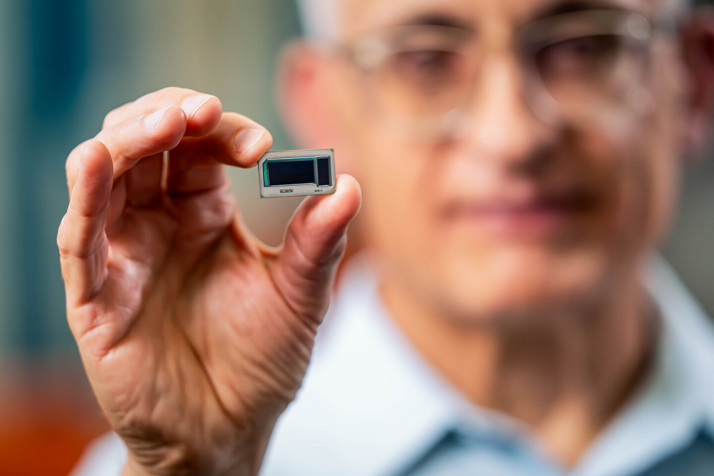
Samsung Accelerates R&D of Glass Substrate Chip Packaging
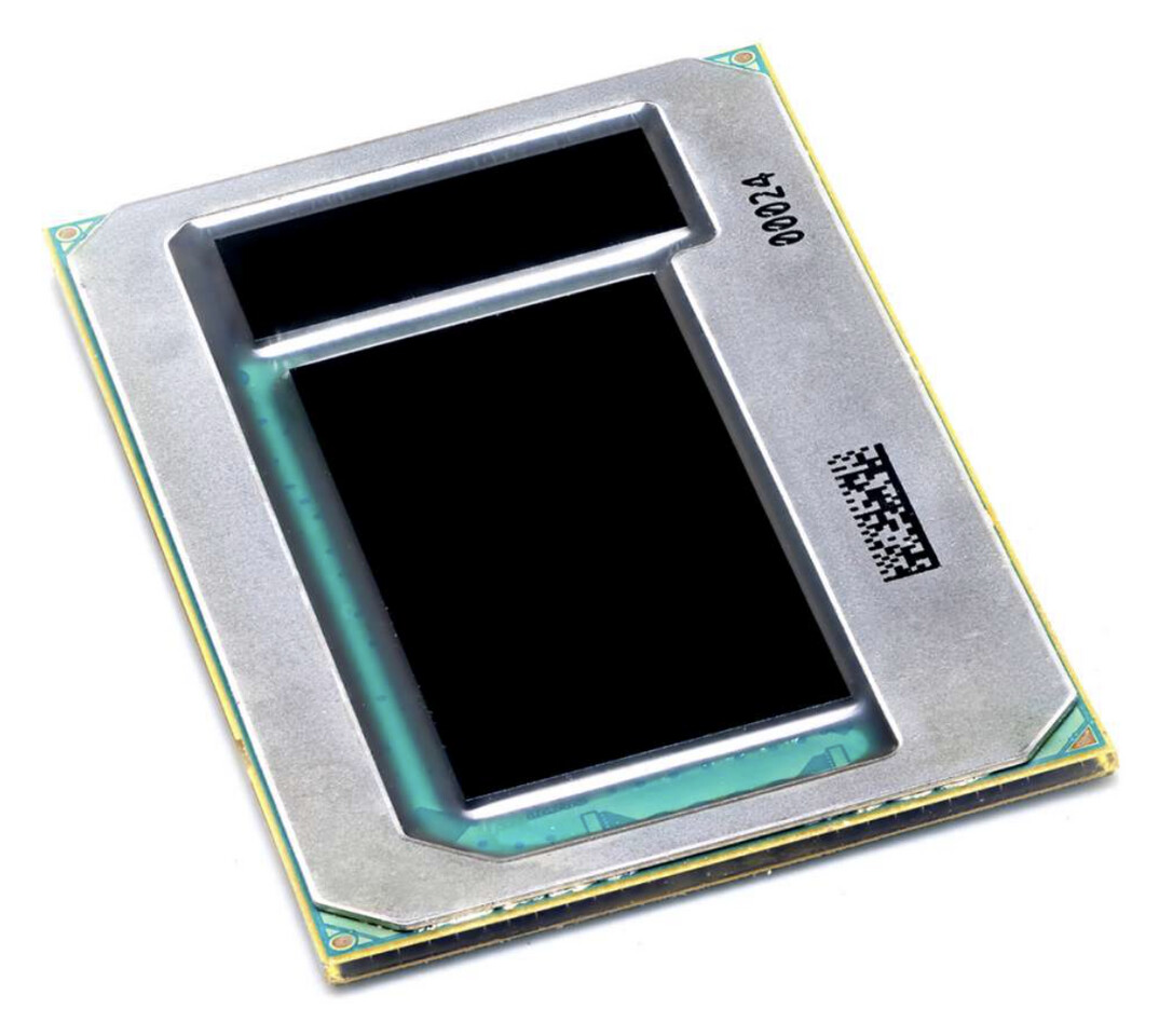
The Samsung Group has formed a new cross-department alliance—according to South Korea's Sedaily—this joint operation will concentrate on the research and development of a "dream substrate." The company's Electronics, Electrical Engineering, and Display divisions are collaborating in order to accelerate commercialization of "glass substrate" chip packaging. Last September, Intel revealed its intention to become an industry leader in "glass substrate production for next-generation advanced packaging." Team Blue's shiny new Arizona fabrication site will be taking on this challenge, following ten years of internal R&D work. Industry watchdogs reckon that mass production—in North America—is not expected to kick off anytime soon. Sensible guesstimates suggest a start date somewhere in 2030.
The Sedaily article states that Samsung's triple department alliance will target "commercialization faster than Intel." Company representatives—in attendance at CES 2024—set a 2026 window as their commencement goal for advanced glass substrate chip package mass production. An unnamed South Korean industry watcher has welcomed a new entrant on the field: "as each company possesses the world's best technology, synergies will be maximized in glass substrate research, which is a promising field...it is also important to watch how the glass substrate ecosystem of Samsung's joint venture will be established." Glass substrate packaging is ideal for "large-area and high-performance chip combinations" due to inherent heat-resistant properties and material strength. So far, the semiconductor industry has struggled with its development—hence the continued reliance on plastic boards and organic materials.


The Sedaily article states that Samsung's triple department alliance will target "commercialization faster than Intel." Company representatives—in attendance at CES 2024—set a 2026 window as their commencement goal for advanced glass substrate chip package mass production. An unnamed South Korean industry watcher has welcomed a new entrant on the field: "as each company possesses the world's best technology, synergies will be maximized in glass substrate research, which is a promising field...it is also important to watch how the glass substrate ecosystem of Samsung's joint venture will be established." Glass substrate packaging is ideal for "large-area and high-performance chip combinations" due to inherent heat-resistant properties and material strength. So far, the semiconductor industry has struggled with its development—hence the continued reliance on plastic boards and organic materials.