 106
106
AMD Radeon RX Vega 56 8 GB Review
Test Setup »PCB Analysis
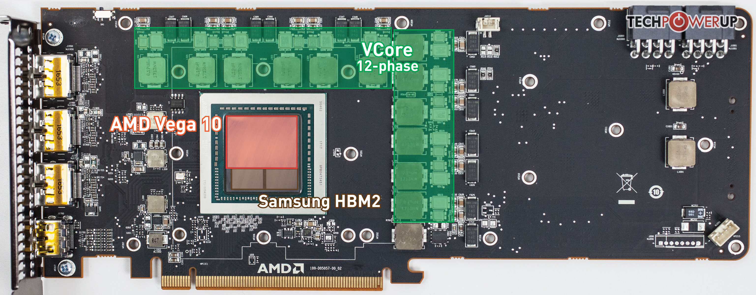
HBM memory integrates tightly with the GPU die, by sitting right next to it on the silicon package. This approach promises smaller PCB real estate usage, but AMD has opted to keep their card full size. Arranged around the GPU is almost nothing but voltage regulation circuitry, probably to keep sufficient space for the heatsink and fan.
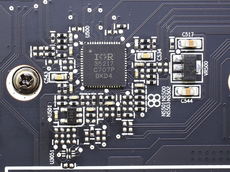


The IR35217 voltage controller seems to be a new design for RX Vega. It feeds its six PWM phase signals into six IR 3598 phase doublers which are located on the backside of the PCB. These six chips now drive twelve power phases, each made up of an IR6894 and IR6211.
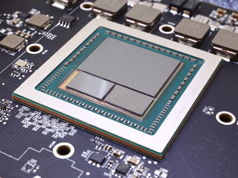
The HBM2 memory chips are made by Samsung. You see two stacks, which add up to a total memory capacity of 8 GB. If you take a closer look at the picture above, you will see empty space between each of the dies. This space is not present on the Radeon RX Vega 64, where the gaps have been filled up with a clear/grey substance. A hint to these differences could be the "made in Taiwan" print on the GPU of Vega 64, whereas Vega 56 uses a GPU "made in Korea".


AMD's Vega 10 graphics processor is produced on a 14 nanometer process, using 12 billion transistors occupying a die size of 486 mm².
May 2nd, 2024 02:15 EDT
change timezone
Latest GPU Drivers
New Forum Posts
- What's your latest tech purchase? (20404)
- Are all software/scheduling issues with e-cores fixed on Intel 12th to 14th Gen - Willing to give hybrid ach a chance now (80)
- 14900k - Tuned for efficiency - Gaming power draw (347)
- TPU's Nostalgic Hardware Club (18486)
- Current Sales, Bundles, Giveaways (10221)
- Throttlestop stopped working (VBS is disabled) (3)
- 7800XT Issue , amdflash bios (9)
- Arctic MX-6 shelf life is just a couple months? (72)
- AMD RX 7000 series GPU Owners' Club (1092)
- Your PC ATM (34536)
Popular Reviews
- Ugreen NASync DXP4800 Plus Review
- HYTE THICC Q60 240 mm AIO Review
- Montech Sky Two GX Review
- Upcoming Hardware Launches 2023 (Updated Feb 2024)
- MOONDROP x Crinacle DUSK In-Ear Monitors Review - The Last 5%
- Team Group T-Force Vulcan ECO DDR5-6000 32 GB CL38 Review
- AMD Ryzen 7 7800X3D Review - The Best Gaming CPU
- ASRock NUC BOX-155H (Intel Core Ultra 7 155H) Review
- Thermalright Phantom Spirit 120 EVO Review
- ASUS Radeon RX 7900 GRE TUF OC Review
Controversial News Posts
- Intel Statement on Stability Issues: "Motherboard Makers to Blame" (219)
- Windows 11 Now Officially Adware as Microsoft Embeds Ads in the Start Menu (159)
- Sony PlayStation 5 Pro Specifications Confirmed, Console Arrives Before Holidays (117)
- AMD's RDNA 4 GPUs Could Stick with 18 Gbps GDDR6 Memory (109)
- NVIDIA Points Intel Raptor Lake CPU Users to Get Help from Intel Amid System Instability Issues (106)
- AMD "Strix Halo" Zen 5 Mobile Processor Pictured: Chiplet-based, Uses 256-bit LPDDR5X (103)
- TechPowerUp Hiring: Reviewers Wanted for Motherboards, Laptops, Gaming Handhelds and Prebuilt Desktops (93)
- AMD Ryzen 9 7900X3D Now at a Mouth-watering $329 (93)