 106
106
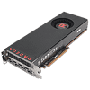
AMD Radeon RX Vega 56 8 GB Review
(106 Comments) »Introduction
The AMD Vega graphics architecture has been grabbing headlines for well over a year now and finally makes its debut in the consumer-segment with the Radeon RX Vega series. When AMD launched its "Polaris" architecture with the Radeon RX 480, which could at best compete with upper-mainstream graphics cards from NVIDIA, such as the GeForce GTX 1060, consumers were half-expecting Vega to be just around the corner, but were put through another year's wait. It's finally here, as the $499 Radeon RX Vega 64, and its little, more exciting sibling, the $399 RX Vega 56.
It appears as if the launch of the Radeon RX Vega series took longer than it did because it's been over two years since AMD's last high-end graphics card launch. The company launched the Radeon R9 Fury series in mid-2015, but has since left the market segment unattended. NVIDIA dominated several key price points, including the $399 point with its GTX 1070, $499 with its GTX 1080, and $649 with its GTX 1080 Ti, and its TITAN series SKUs well above the $1000 mark. The $399 performance-segment price point has been particularly important for both NVIDIA and AMD, and how AMD has left it unattended has been quite surprising. We can't imagine that it would have been difficult to build a slightly bigger "Polaris" based GPU with conventional technologies, such as GDDR5 memory, to take a swing at the $399 price-point; at least now, AMD has something to compete with in the Radeon RX Vega 56. AMD has greatly simplified its nomenclature with the RX Vega series. The term "Vega" signifies the architecture on which the GPU is based on, and the number after that signifies the compute unit (CU) count.

"Vega 10" is a multi-chip module, much like "Fiji," which powered the R9 Fury series. It combines a large GPU die based on the Vega architecture with two HBM2 memory stacks. On the RX Vega series, there is 8 GB of total memory; while on some of the Pro Vega SKUs, the chip has 16 GB of it. AMD is referring to this memory as "High Bandwidth Cache," with the operative term being "cache" as opposed to "memory." This is because of sweeping changes the company brought about in the way the GPU addresses video memory. The GPU features a large virtual address-space spanning several terabytes, where a small portion of it is physical and the GPU juggles "hot data" (most frequently accessed data) in and out of it. With this, AMD claims to overcome many of the fundamental memory-management issues that had been inherent to its Graphics CoreNext architecture, which it had been working around by throwing brute memory bus width and data compression at it.
The Radeon RX Vega 56 features 56 of the 64 next-generation Compute Units (NGCUs) present on the "Vega 10" silicon, which works out to a stream processor count of 3,584. This proportionately lowers the TMU count to 224. The ROP count is left untouched, at 64. The card features 8 GB of HBM2 memory across a 2048-bit wide memory interface. AMD has also tempered down clock speeds a bit, with its core running at up to 1156 MHz and memory at 800 MHz, yielding a memory bandwidth of 409 GB/s, less than the 484 GB/s of the RX Vega 64. This dialing down of clock speeds may have had a profound impact on energy efficiency, and if the performance lives up, AMD could finally have a price-performance sweetspot product to take on the GTX 1070, given its $399 price.
We put the RX Vega 56 through our vast and modern test bench and had it compete against key NVIDIA SKUs, such as the GTX 1060 6 GB, GTX 1070, GTX 1080, and GTX 1080 Ti; at resolutions as high as 4K Ultra HD. If this SKU can tame 4K, it will be the first AMD GPU to do so.
| GeForce GTX 980 Ti | Radeon R9 Fury X | GeForce GTX 1070 | Radeon RX Vega 56 | GeForce GTX 1080 | Radeon RX Vega 64 | Radeon RX Vega 64 Liquid | GeForce GTX 1080 Ti | |
|---|---|---|---|---|---|---|---|---|
| Shader Units | 2816 | 4096 | 1920 | 3584 | 2560 | 4096 | 4096 | 3584 |
| ROPs | 96 | 64 | 64 | 64 | 64 | 64 | 64 | 88 |
| Graphics Processor | GM200 | Fiji | GP104 | Vega 10 | GP104 | Vega 10 | Vega 10 | GP102 |
| Transistors | 8000M | 8900M | 7200M | 12500M | 7200M | 12500M | 12500M | 12000M |
| Memory Size | 6 GB | 4 GB | 8 GB | 8 GB | 8 GB | 8 GB | 8 GB | 11 GB |
| Memory Type | GDDR5 | HBM | GDDR5 | HBM2 | GDDR5X | HBM2 | HBM2 | GDDR5X |
| Memory Bus Width | 384 bit | 4096 bit | 256 bit | 2048 bit | 256 bit | 2048 bit | 2048 bit | 352 bit |
| Core Clock | 1000 MHz+ | 1050 MHz | 1506 MHz+ | 1156 MHz+ | 1607 MHz+ | 1274 MHz+ | 1406 MHz+ | 1481 MHz+ |
| Memory Clock | 1750 MHz | 500 MHz | 2002 MHz | 800 MHz | 1251 MHz | 953 MHz | 953 MHz | 1376 MHz |
| Price | $390 | $380 | $350 | $400 | $500 | $500 | $700 | $700 |
Architecture
As we mentioned in the introduction, when the Radeon RX 480 turned out to be an upper-mainstream product in June 2016, consumers half-expected the performance-thru-enthusiast segment "Vega" to launch by the end of the year. That didn't happen. What we got instead were not one, but two media events detailing the "Vega" architecture. On each occasion, we did a special article detailing the press-decks given to us by AMD. Our first article, dated early-January, focused on the broader points of the architecture. Our second article followed close to seven months later, getting into the finer points of the architecture. On this page, we'll summarize the most important bits of content from both presentations.

The Radeon RX Vega 56 is based on the "Vega 10" GPU. This is a multi-chip module of a GPU die, and memory stacks, much like its logical predecessor, "Fiji" (R9 Fury X, R9 Nano). The GPU die is built on the 14 nm FinFET process and packs over 12 billion transistors. It's wired to two 32 Gbit HBM2 memory stacks over a 2048-bit wide memory interface, which is half the bus width of "Fiji", but is somewhat made up for with higher clocks. The bandwidth itself is less than that of the R9 Fury, at just 484 GB/s against the Fury's 512 GB/s, but AMD made some sweeping changes to the way in which it addresses memory, which should more than make up for the bandwidth deficit.


Memory-management has traditionally been a problem area for AMD's otherwise stellar Graphics CoreNext architecture, and AMD added raw bus width and memory compression to overcome issues that were intrinsic to the architecture. With Vega, AMD is addressing those fundamental issues by using a memory concept called "High Bandwidth Cache," with the keyword being "cache." The "Vega" silicon addresses a large virtual-memory space that spans up to 512 TB, a tiny portion of which is physical, in this case the "cache." This allows for the fine-grained movement of data in and out of the virtual-address space based on data "heat" (frequency of access).


The essential hierarchy of the GPU doesn't appear to have changed with "Vega"; however, its designers seem to have made big changes with the front-end and back-ends of the rendering pipeline, while incrementally improving the Compute Units, the number-crunching components that do the heavy lifting.
The newer-generation programmable geometry pipeline provides double the throughput over the previous generation. The Next-Generation Compute Units (NGCUs) are based on the 5th generation Graphics CoreNext architecture and feature support for not just FP16 operations (introduced with "Polaris"), but also primitive 8-bit operations. Bolstered by Rapid Packed Math, each CU can handle up to 512 8-bit operations per clock cycle, and up to 256 16-bit ones. Quite a few of today's effects can be simplified to 16-bit or 8-bit ops, which frees up much of the CU's resources for other ops. Lastly, there is an improved pixel-engine, featuring a draw-binning rasterizer.


The "Vega 10" silicon features 64 NGCUs, each with 64 stream processors (SP), indivisible SIMD units which total the chip's SP count at 4,096 on the RX Vega 64 and 3,584 on the RX Vega 56, since it only has 56 out of the 64 CUs enabled. The chip also features 256 texture memory units (TMUs) and 64 ROPs. Its 2048-bit wide HBM2 memory interface holds 8 GB of memory (or high-bandwidth cache) on the Radeon RX Vega 64 and RX Vega 56.
AMD Enhanced Sync
We can safely call the AMD FreeSync technology the victor of the adaptive display-sync-standard war. It beats G-SYNC because it's both easy and free to implement and has the backing of VESA, the display-standards governing body. AMD is doubling down on adaptive display-sync with a new standard, Enhanced Sync, which is bound to be more successful because it doesn't even need compatibility on the monitor's side, and since it works with any digital display connector.
Before we get to the mechanics of Enhanced Sync, here's a quick refresher about V-Sync. Your display has a fixed maximum refresh rate (the rate at which it draws a new frame to make up moving images), while your PC puts out frames to the display at a variable rate, depending on the speed of your hardware. If it puts out frames at a rate slower than your monitor's refresh-rate, you experience stuttering (a noticeably rough video). If it puts out at a higher rate, you experience screen tearing, caused because your GPU is pumping in new frames before your monitor can finish drawing frames at its rate. V-Sync is a feature in which the software limits the rate at which your GPU puts out frames, by syncing it with the refresh-rate of your display. The result is smooth display, but it results in a lot of your frames getting culled, and causes input lag because your game only takes in the same number of inputs per second as the number of frames it has to draw per second.


AMD feels that there is a middle path for games that don't have FreeSync-ready displays, and yet want to counter page-tearing at high frame rates or stuttering at low frame rates - hence Enhanced Sync. This is not meant as a replacement, successor, or substitute to FreeSync, but, rather, as its next best thing.
Enhanced Sync counters page tearing by allowing your game to think it has no V-Sync frame-rate caps, thereby taking in unlimited amount of inputs per second while, on the other hand, intelligently culling the number of frames being sent to the display (and conserving hardware resources in the process), so that the output looks in-sync, without the appearance of lost frames, torn-frames, or other artifacts. Enhanced Sync combats the problem of low frame rates causing stuttering by allowing for some frame tearing.
FreeSync
FreeSync provides a novel solution to the problem of low frame rates causing display stutter, by keeping your monitor in sync with the frame rate of your game in real time, rather than the other way around. The display's refresh rate is controlled by the source (in this case, your GPU) rather than it having a static refresh rate. When your game's frame rate is higher than the refresh rate of your display, beyond a point, FreeSync allows the game to take in a limitless amount of input, while running the display at its highest refresh rate and culling frames being sent to it. The display's refresh rate keeps in sync with your software fluidly, and hence gives you the appearance of fluid motion, and an uncompromising game-input experience.Our Patreon Silver Supporters can read articles in single-page format.
Apr 23rd, 2024 12:58 EDT
change timezone
Latest GPU Drivers
New Forum Posts
- What's an inexpensive AIO product line with a strong pump and low price? (77)
- Embracer Group is breaking into 3 smaller companies... lol who saw this coming, what a joke (8)
- Cinebench crashed my PC. My Wi-Fi stopped working, and I keep getting a "Please wait" screen when I boot up my PC. (24)
- Which new games will you be buying? (295)
- Unlock the shaders - AMD Radeon RX 560D (324)
- What's your latest tech purchase? (20299)
- FINAL FANTASY XIV: Dawntrail Official Benchmark (67)
- Is there a technical reason that Windows 11 doesn't have built into it battery charge limitation? (30)
- Asus Crosshair X670E - CPU Package temps (10)
- Core PL1 + GPU PL1 + Ring EDP OTHER (4)
Popular Reviews
- Horizon Forbidden West Performance Benchmark Review - 30 GPUs Tested
- Fractal Design Terra Review
- Corsair 2000D Airflow Review
- Thermalright Phantom Spirit 120 EVO Review
- Minisforum EliteMini UM780 XTX (AMD Ryzen 7 7840HS) Review
- ASUS GeForce RTX 4090 STRIX OC Review
- NVIDIA GeForce RTX 4090 Founders Edition Review - Impressive Performance
- ASUS GeForce RTX 4090 Matrix Platinum Review - The RTX 4090 Ti
- Creative Pebble X Plus Review
- MSI GeForce RTX 4090 Gaming X Trio Review
Controversial News Posts
- Sony PlayStation 5 Pro Specifications Confirmed, Console Arrives Before Holidays (116)
- NVIDIA Points Intel Raptor Lake CPU Users to Get Help from Intel Amid System Instability Issues (105)
- AMD "Strix Halo" Zen 5 Mobile Processor Pictured: Chiplet-based, Uses 256-bit LPDDR5X (101)
- US Government Wants Nuclear Plants to Offload AI Data Center Expansion (98)
- Windows 10 Security Updates to Cost $61 After 2025, $427 by 2028 (84)
- Developers of Outpost Infinity Siege Recommend Underclocking i9-13900K and i9-14900K for Stability on Machines with RTX 4090 (82)
- TechPowerUp Hiring: Reviewers Wanted for Motherboards, Laptops, Gaming Handhelds and Prebuilt Desktops (74)
- Intel Realizes the Only Way to Save x86 is to Democratize it, Reopens x86 IP Licensing (70)