 223
223
AMD Radeon Vega GPU Architecture
Next Generation Geometry and Compute »Improved Memory Mangement

Take a good look at the schematic diagram above. It is not a die block diagram, it's not even the layout of the multi-chip module that some of the first "Vega" GPUs will be, but rather illustrates a completely revamped memory architecture which makes sure data moves smoothly in and out of the GPU, and precious resources aren't wasted in fetching data from the host machine. AMD GPUs have traditionally been endowed with vast amounts of memory bandwidth using wide memory bus widths; however, AMD thinks there is room for improvement in the way the GPU juggles data between the host and its local video memory, and that it can no longer simply throw brute memory bandwidth at some fundamental problems.

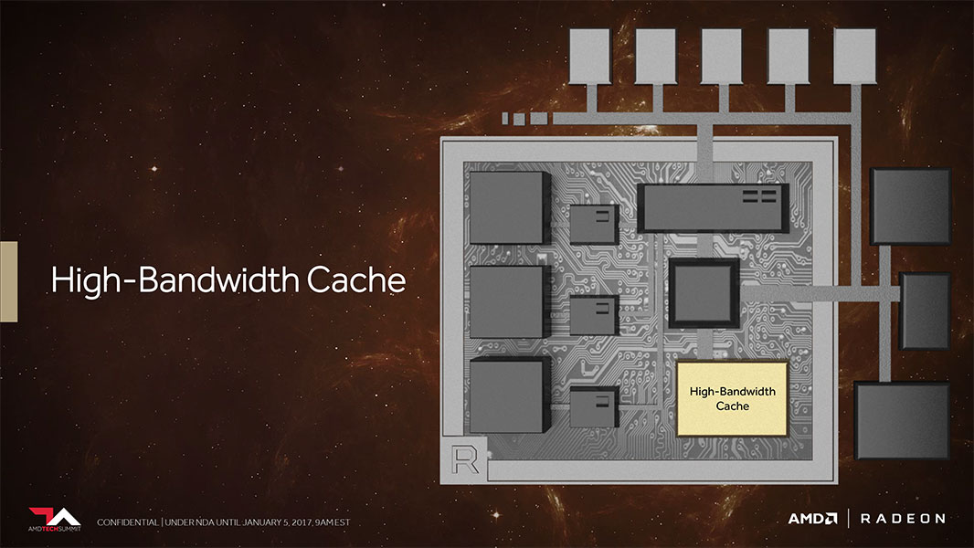
AMD feels there is a disparity between the memory allocation and actual memory access by apps. An app could load into memory resources it finds relevant to the 3D scene being rendered, but not actually access all of it all the time. This disparity eats up precious memory, hogs memory bandwidth, and wastes clock cycles in trying to move data. The graphics driver development team normally collaborates with game developers to minimize this phenomenon and rectify it both through game patches and driver updates. AMD feels something like this can be corrected at the hardware level. AMD calls this "adaptive fine-grained data movement." It is a comprehensive memory allocation pipeline that senses the relevance of data to preemptively move it to the relevant physical memory, or defers access.


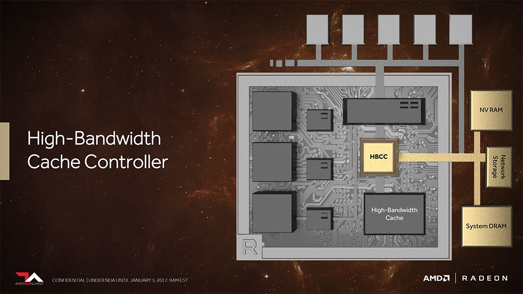
Pulling something like this off requires new hardware components not found on AMD GPUs ever before. It begins with a fast cache memory that sits at a level above the traditional L2 cache, one that is sufficiently large and has extremely low latency. This cache is a separate silicon die that sits on the interposer, the silicon substrate that connects the GPU die to the memory stacks. AMD is calling this the High Bandwidth Memory Cache (HBMC). The GPU's conventional memory controllers won't interface with this cache since a dedicated High Bandwidth Cache Controller (HBCC) on the main GPU die handles it. High Bandwidth Memory Cache isn't the same as the HBM2 memory stacks.
The HBCC has direct access to the other memory along the memory pipeline, including the video memory, system memory, and so on. It has its own 512 TB virtual address space that's isolated / abstract from the machine's general address space. The GPU uses the HBMC to cushion and smooth out data movement between the host machine and the GPU. This approach ensures the GPU has to spend lesser resources on fetching irrelevant data, which greatly improves memory bandwidth utilization. The reason for such a large virtual address space is the same as on the CPU: Adresses can be allocated more efficiently, with the memory-management unit in the GPU managing the virtual-to-physical mapping and also having the ability to move memory pages between storage layers, similar to how the Windows paging file works. Also, you'll notice the little box named "NVRAM." This means the GPU has the ability to directly interface with NAND Flash or 3D X-point SSDs over a localized PCIe connection, which gives it a fast scratchpad for help with processing gargantuan data sets. The "Network" port lets graphics card makers add network PHYs directly onto the card, which would help with rendering farms. This way, AMD is prepping a common silicon for various applications (consumer graphics, professional graphics, and rendering farms).

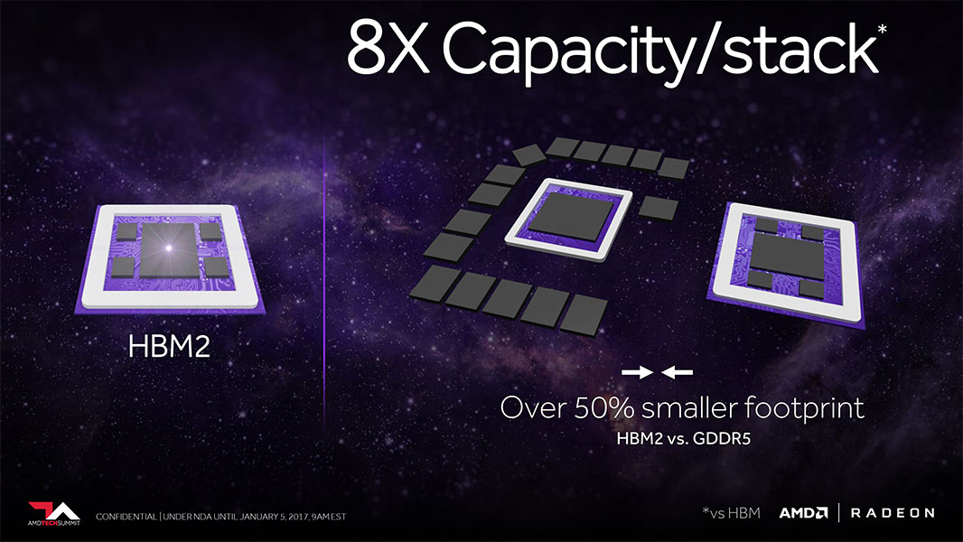
As reported in the news, "Vega" takes advantage of HBM2 memory, which comes with eight times the maximum density per stack and double the bandwidth as HBM1 memory, which debuted with the Radeon R9 Fury X. In theory, you can deploy up to 32 GB of memory across four stacks, doing away with the crippling 4 GB limitation of HBM1.
Apr 25th, 2024 22:19 EDT
change timezone
Latest GPU Drivers
New Forum Posts
- What are you playing? (20530)
- Secure boot already open help (0)
- TPU's Nostalgic Hardware Club (18465)
- Post your Speedometer 3.0 Score (36)
- Size on Disk Excessively Different than Size (9)
- Dell Workstation Owners Club (3056)
- Core PL1 + GPU PL1 + Ring EDP OTHER (10)
- Best SSD for system drive (80)
- Which new games will you be buying? (315)
- BSOD if I touch the pcache offset voltage in throttlestop (i9-13900hx lenovo pro 7i) (23)
Popular Reviews
- Fractal Design Terra Review
- Thermalright Phantom Spirit 120 EVO Review
- Corsair 2000D Airflow Review
- ASUS GeForce RTX 4090 STRIX OC Review
- NVIDIA GeForce RTX 4090 Founders Edition Review - Impressive Performance
- ASUS GeForce RTX 4090 Matrix Platinum Review - The RTX 4090 Ti
- MSI GeForce RTX 4090 Suprim X Review
- Gigabyte GeForce RTX 4090 Gaming OC Review
- MSI GeForce RTX 4090 Gaming X Trio Review
- MSI GeForce RTX 4090 Suprim Liquid X Review
Controversial News Posts
- Sony PlayStation 5 Pro Specifications Confirmed, Console Arrives Before Holidays (117)
- Windows 11 Now Officially Adware as Microsoft Embeds Ads in the Start Menu (108)
- NVIDIA Points Intel Raptor Lake CPU Users to Get Help from Intel Amid System Instability Issues (106)
- AMD "Strix Halo" Zen 5 Mobile Processor Pictured: Chiplet-based, Uses 256-bit LPDDR5X (101)
- US Government Wants Nuclear Plants to Offload AI Data Center Expansion (98)
- AMD's RDNA 4 GPUs Could Stick with 18 Gbps GDDR6 Memory (88)
- Developers of Outpost Infinity Siege Recommend Underclocking i9-13900K and i9-14900K for Stability on Machines with RTX 4090 (85)
- Windows 10 Security Updates to Cost $61 After 2025, $427 by 2028 (84)