AMD Ryzen 3 3100 Review - Disruptive Price/Performance 15

AMD Ryzen 3 3100 Review - Disruptive Price/Performance

Test Setup »

Architecture

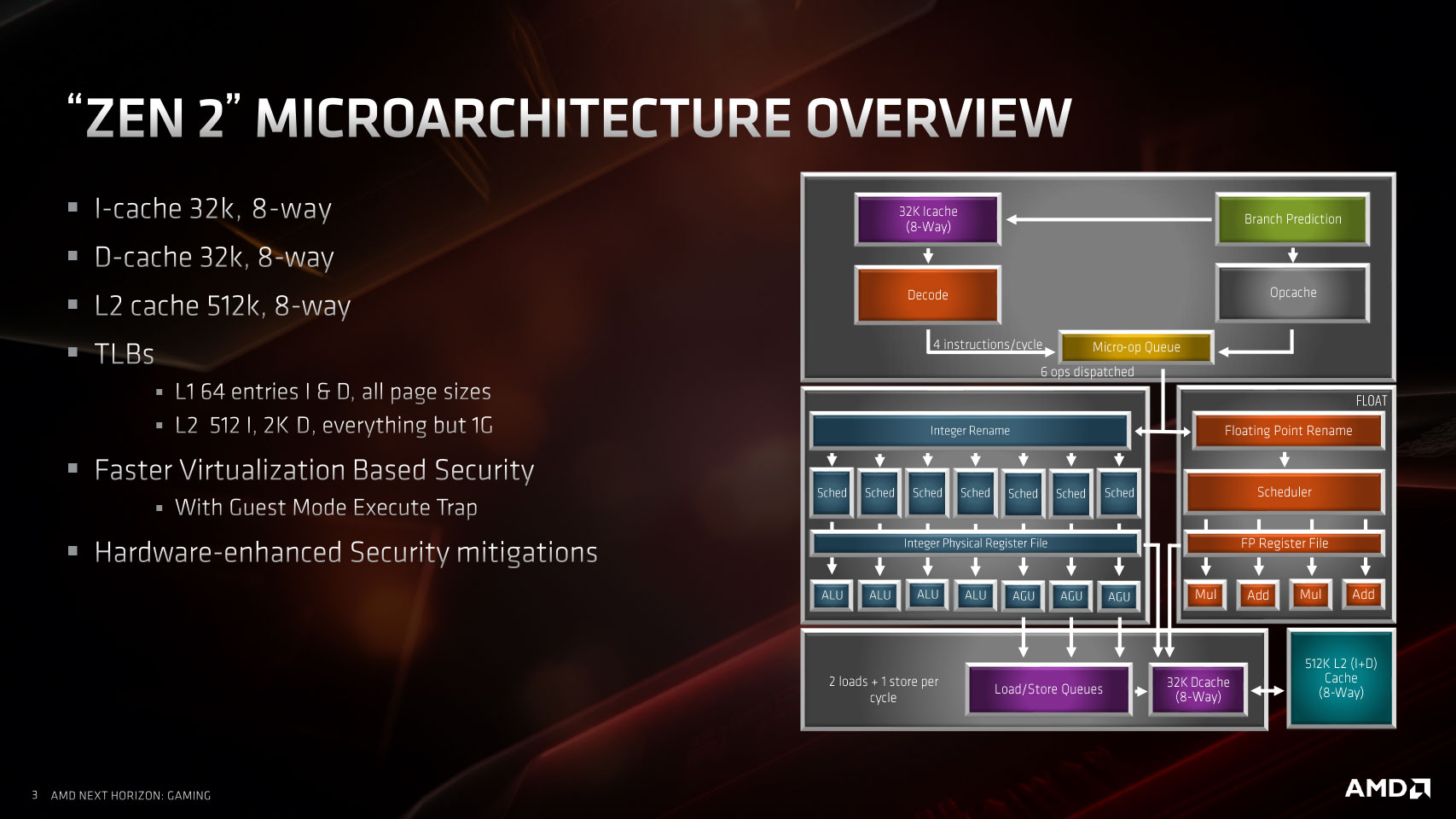
The architecture is no different from the Ryzen 9 3950X or any other "Matisse," so you can click on the button below to read about it, or skip that section if you're familiar with it.

AMD Zen 2 Microarchitecture Brief

The AMD Zen 2 Microarchitecture


AMD's 3rd generation Ryzen processors use the "Zen 2" microarchitecture. The 2nd generation Ryzen chips use an enhanced first-generation "Zen" derivative called "Zen+," which has process and boost algorithm improvements eke out roughly a 4% IPC uplift. With "Zen 2," AMD's key design goal is to finally beat Intel in the IPC game. IPC, or instructions per clock, is loosely used to denote a CPU core's performance at a given clock speed. For the past 15 or so years, Intel dominated AMD at IPC, while AMD attempted to make their processors competitive by cramming in more CPU cores than Intel at any given price point for competitive multi-threaded performance. Today's software environment is increasingly multi-threaded, as are games. With "Zen 2," AMD set itself an ambitious double-digit-percentage IPC uplift target to catch up or overtake Intel's latest "Coffee Lake" microarchitecture at IPC. AMD didn't stop there and even increased core counts for the platform at higher price points. The 3rd generation Ryzen family even includes a 16-core processor, which is a tremendous core count for the mainstream desktop platform.


Before we get into the interesting and quirky way AMD crammed 16 cores into this chip, let's talk about the "Zen 2" CPU core. After the colossal failure that was "Bulldozer," AMD set out to once again build strong and monolithic CPU cores that share nothing except L3 cache with other cores. It achieved this desired result with "Zen," which posted a mammoth 40%–50% IPC increase over "Bulldozer," catapulting AMD back into competitiveness. "Zen" cores IPC sits somewhere between "Haswell" and "Skylake/Coffee Lake," which was enough for AMD as it backed the IPC increase with higher core counts compared to Intel. Over the 8th and 9th generations of Core processors that retained the same IPC as "Skylake", Intel shored up core counts to match AMD. Wanting to set up a definitive edge over Intel, AMD not only worked to increase IPC, but also core counts.

The "Zen 2" CPU core has essentially the same component layout and hierarchy as "Zen," but with major changes and broadening of key components. As with "Zen" (or most x86 CPU cores), the "Zen 2" core is made up of five key components: Fetch, Decode, Integer, Floating-point, and Load/Store. Fetch and Decode tell the CPU core what needs to be done and what data or instructions are needed; Integer and Floating-point Unit execute a mathematical model of what needs to be done depending on the data type and nature of the instruction; Load/Store are the I/O of the CPU core. At various levels, there are tiny buffers, registers that store instructions, and larger caches that cushion data-transfers between various components.


AMD updated the Fetch and Decode units, which contribute to IPC, by making the CPU work "smarter." The updated Integer and FPU make the CPU work "harder," the Load/Store unit's job is to make sure the other components aren't starved for things to do. The Fetch unit is updated with a TAGE branch predictor. Invented in 2006, TAGE is considered the best branch-prediction technique by the IEEE. AMD broadened the BTB (branch target buffers) at L1 and L2 by doubling the L1 entries to 512k, and L2 entries to 7,000 from 4,000. The ITA (indirect target array) has also been expanded. The design goal for updating the Fetch unit is to lower "mispredictions" (bad guesses) that wasted load/storage operations by 30 percent. The 32 KB L1 instruction cache has also been improved. The Decode unit has two improvements to the Op cache: improved instruction fusion and the ability to push up to 4,000 fused instructions per clock cycle.


We now move on to the two components that contribute the most to the IPC, the Integer and Floating-point Units. The Integer unit receives incremental updates in the form of a broader integer scheduler that handles 92 entries (up from 84), with four 16-entry ALU queues and one 28-entry AGU queue. The general-purpose physical register file has now been expanded to 180 entries from 168. The issue-per-cycle has been broadened to 7 from 6, which now includes 4 ALUs and 3 AGUs. The reorder-buffer (ROB) has been broadened to 224 entries, up from 192. The SMT (simultaneous multi-threading) logic has been tweaked to better share the ALUs and AGUs among the logical processors. The FPU has the bulk of the innovation with "Zen 2." The load/store bandwidth of the FPU has been doubled to 256-bit, up from 128-bit on "Zen."

The core now also supports a sort of AVX-256: AVX/AVX2-flagged instructions with 256-bit registers. There are many applications for this, such as physics simulation, audio-stack execution, and memory-copy performance improvement. Multiplication operation latency has been improved by 33 percent.


Lastly, we have the Load/Store unit with a similar round of generational enhancements. The entry-store queue is expanded to 48 entries, up from 44. The L2 TLB (translation lookaside buffer) has been expanded by 33% to 2,000 entries, and its latency improved. The 32 KB L1 Data cache has two 256-bit read paths and one 256-bit write path, with 64-byte load and 32-byte store alignment boundaries. The load/store bandwidth to L2 has been doubled to 32 bytes per clock.


We now move on to the cache hierarchy, which is essentially the same as "Zen." Notwithstanding the technical changes described above, the "Zen 2" core still has a 32 KB 8-way L1I cache, a 32 KB 8-way L1D cache, and a dedicated 512 KB 8-way L2 cache. AMD doubled the shared L3 cache size to 16 MB. Every CCX (quad-core compute complex) on a "Zen 2" processor now has 16 MB of shared L3 cache. The doubling in L3 cache size was necessitated not just by Intel sharing larger amounts of L3 cache among individual cores on the "Coffee Lake Refresh" silicon (16 MB shared among all 8 cores), but also because the larger L3 cache on a "Zen 2" CCX cushions data transfers with the I/O controller die.


This brings us to the interesting and quirky way AMD achieved 16 cores. The Ryzen 9 3900X and Ryzen 5 3600 processor packages are codenamed "Matisse." This is a multi-chip module (MCM) of one or two 7 nm 8-core "Zen 2" CPU chiplets and one I/O controller die built on the 12 nm process. AMD made sure only those components that tangibly benefit from the shrink to 7 nm—namely, the CPU cores—are built on the new process, while those components that don't benefit from 7 nm stay on the existing 12 nm process, on the I/O controller die. AMD carved the Ryzen 5 3600 out by using just one "Zen 2" chiplet and enabling 6 cores on it, 3 per CCX.


These components include the processor's dual-channel DDR4 memory controller, a 24-lane PCI-Express gen 4.0 root-complex, and an integrated southbridge that puts out some platform connectivity directly from the AM4 socket, such as SATA 6 Gbps and USB 3.1 ports. Infinity Fabric is the interconnect that binds the three dies by providing a 100 GB/s data path between each CPU chiplet and the I/O controller. The memory clock is now practically de-coupled from the Infinity Fabric clock, which should improve memory overclocking headroom. AMD also claims to have put a lot of work into improving memory-module compatibility across brands, especially since Samsung stopped mass-production of the expensive B-die DRAM chip that favored AMD processors. The memory scaling article talks a little more about this.

Architectural Innovations Specific to Ryzen 3 3300X and 3100

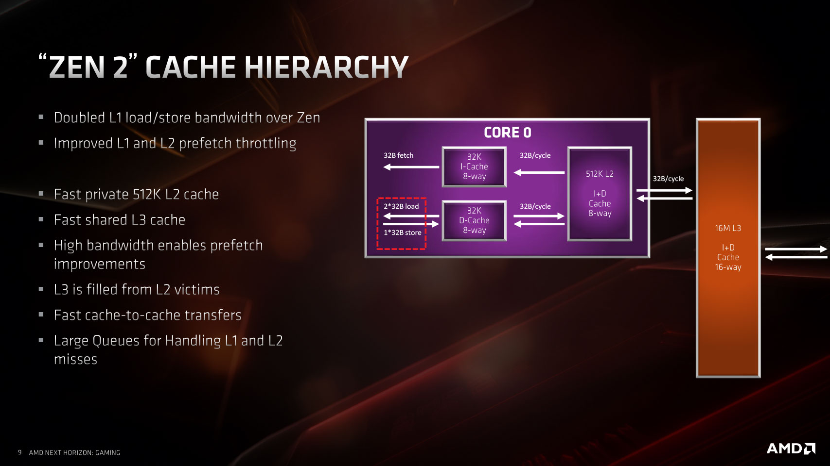
Both the Ryzen 3 3300X and Ryzen 3 3100 are 4-core/8-thread parts, but their segmentation goes beyond clock speeds to justify the 20% price gap between them. AMD tapped into the multi-core topology of its "Zen 2" microarchitecture to obtain the 4-core configuration differently between the two SKUs. Each 7 nm "Zen 2" chiplet (CCD) physically features eight CPU cores spread across two CCX (compute complexes) with four cores and 16 MB of L3 cache, each. For the 8-core Ryzen 7 parts, all eight cores are enabled. For the 6-core Ryzen 5 and 12-core dual-chiplet Ryzen 9 3900X, one core per CCX is disabled, yielding a 3+3 core CCX configuration.


The Ryzen 3 3300X and 3100 are designed differently at the CCX-level. For the entry-level 3100, AMD disabled two cores per CCX and reduced the L3 cache amount to 8 MB per CCX. This 2+2 core CCX configuration with 16 MB of L3 cache (2x 8 MB) still qualifies AMD's specs sheet. The 3300X has a key difference. One of the two CCX on the chiplet is completely disabled, and all four cores are localized to a single CCX, with its full 16 MB L3 cache enabled and shared between all four cores. This improves inter-core latency and lets a core access >8 MB of L3 cache if it wants. For the Ryzen 3 3100, inter-core communication between CCXs comes with certain performance costs arising from latency.

AMD B550 Chipset

With premium AMD X570 chipset-based motherboards starting at $150, it's less likely that someone would pair the 3rd gen Ryzen 3 with it. Choosing a cheaper B450 motherboard would mean giving up on killer features such as PCIe gen 4.0. AMD hence launched the new B550 mid-range chipset alongside these processors. Motherboards based on the new chipset are expected to be available around mid June, 2020, at starting prices similar to B450-based ones. The B550 chipset lets you have PCI-Express gen 4.0 connectivity from the "Matisse" processor, while limiting general purpose PCIe downstream connectivity to gen 3.0.


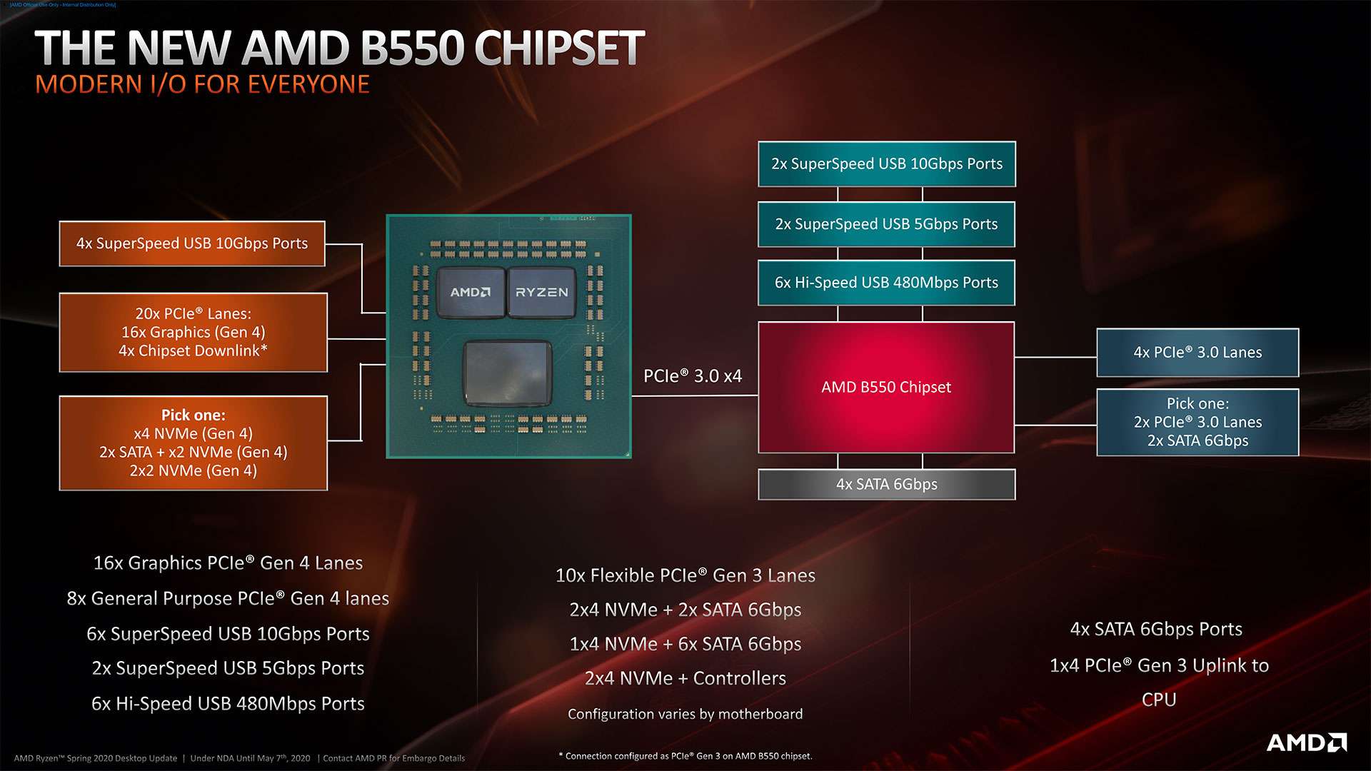
On a typical B550 chipset motherboard, the main PCI-Express x16 slot will be gen 4.0 if paired with a 3rd gen Ryzen "Matisse" processor, as would one of the board's M.2 NVMe slots that's wired to the processor. All other PCIe or M.2 slots which are wired to the B550 chipset will be gen 3.0. This way, future-proofing of the platform for next-generation graphics cards and SSDs remains intact. The B550 chipset provides up to six SATA 6 Gbps ports with AHCI and RAID capability, up to two 10 Gbps USB 3.1 gen 2 ports (in addition to four such ports put out by the "Matisse" processor), two additional USB 3.1 gen 1 ports, and six USB 2.0 ports. The platform's HDA and LPCIO buses are located on the processor.


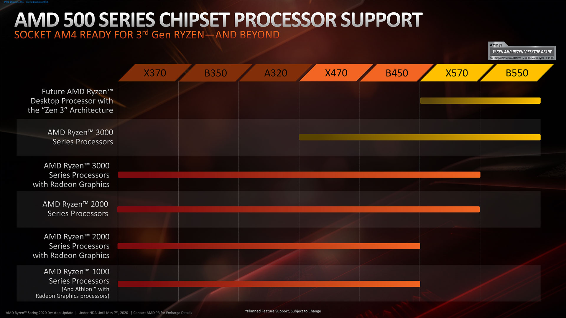
A word on compatibility: the B550 chipset only supports 3rd gen Ryzen "Matisse" processors as of this writing and AMD confirmed support for next-generation processors based on the "Zen 3" architecture. You cannot pair a B550 motherboard with older Ryzen 2000/1000 processors or even the 3200G or 3400G APUs based on the older "Zen+" microarchitecture. There will be clear labeling on B550 chipset motherboard boxes to this effect.

What we like most about the B550 is its low TDP, which lets motherboard designers make do with passive heatsinks; unlike X570, which requires active fan-heatsinks.
Next Page »Test Setup
View as single page
Apr 27th, 2024 01:05 EDT change timezone

New Forum Posts

Popular Reviews

Controversial News Posts