 173
173
AMD Ryzen 9 3900X Review
Test Setup »Architecture
AMD's 3rd generation Ryzen processors use the "Zen 2" microarchitecture. The 2nd generation Ryzen chips use an enhanced first-generation "Zen" derivative called "Zen+", which has process and boost algorithm improvements eke out roughly a 4% IPC uplift. With "Zen 2", AMD's key design goal is to finally beat Intel in the IPC game. IPC, or instructions per clock, is loosely used to denote a CPU core's performance at a given clock speed. For the past 15 or so years, Intel dominated AMD at IPC, while AMD attempted to make their processors competitive by cramming in more CPU cores than Intel at any given price point for competitive multi-threaded performance. Today's software environment is increasingly multi-threaded, as are games. With "Zen 2", AMD set itself an ambitious double-digit-percentage IPC uplift target to catch up or overtake Intel's latest "Coffee Lake" microarchitecture at IPC. AMD didn't stop there and even increased core counts for the platform at higher price points. The 3rd generation Ryzen family even includes a 16-core processor, which is a tremendous core count for the mainstream-desktop platform.


Before we get into the interesting and quirky way AMD crammed 16 cores into this chip, let's talk about the "Zen 2" CPU core. After the colossal failure that was "Bulldozer," AMD set out to once again build strong and monolithic CPU cores that share nothing except L3 cache with other cores. It achieved this desired result with "Zen", which posted a mammoth 40%–50% IPC increase over "Bulldozer", catapulting AMD back into competitiveness. "Zen" cores IPC sits somewhere between "Haswell" and "Skylake/Coffee Lake", which was enough for AMD as it backed the IPC increase with higher core counts compared to Intel. Over the 8th and 9th generations of Core processors that retained the same IPC as "Skylake", Intel shored up core counts to match AMD. Wanting to set up a definitive edge over Intel, AMD not only worked to increase IPC, but also core counts.
The "Zen 2" CPU core has essentially the same component layout and hierarchy as "Zen", but with major changes and broadening of key components. As with "Zen" (or most x86 CPU cores), the "Zen 2" core is made up of five key components: Fetch, Decode, Integer, Floating-point, and load-store. Fetch and Decode tell the CPU core what needs to be done and what data or instructions are needed; Integer and Floating-Point Unit execute a mathematical model of what needs to be done depending on the data type and nature of the instruction; Load/Store are the I/O of the CPU core. At various levels, there are tiny buffers, registers that store instructions, and larger caches that cushion data-transfers between various components.


AMD updated the Fetch and Decode units, which contribute to IPC, by making the CPU work "smarter". The updated Integer and FPU make the CPU work "harder", the Load/Store unit's job is to make sure the other components aren't starved of things to do. The Fetch unit is updated with a TAGE branch predictor. Invented in 2006, TAGE is considered to be the best branch-prediction technique by the IEEE. AMD broadened the BTB (branch target buffers) at L1 and L2 by doubling the L1 entries to 512k, and L2 entries to 7,000 from 4,000. The ITA (indirect target array) has also been expanded. The design goal for updating the Fetch unit is to lower "mispredictions" (bad guesses) that wasted load/storage operations by 30 percent. The 32 KB L1 instruction cache has also been improved. The Decode unit has two improvements to the Op cache: improved instruction fusion and the ability to push up to 4,000 fused instructions per clock cycle.
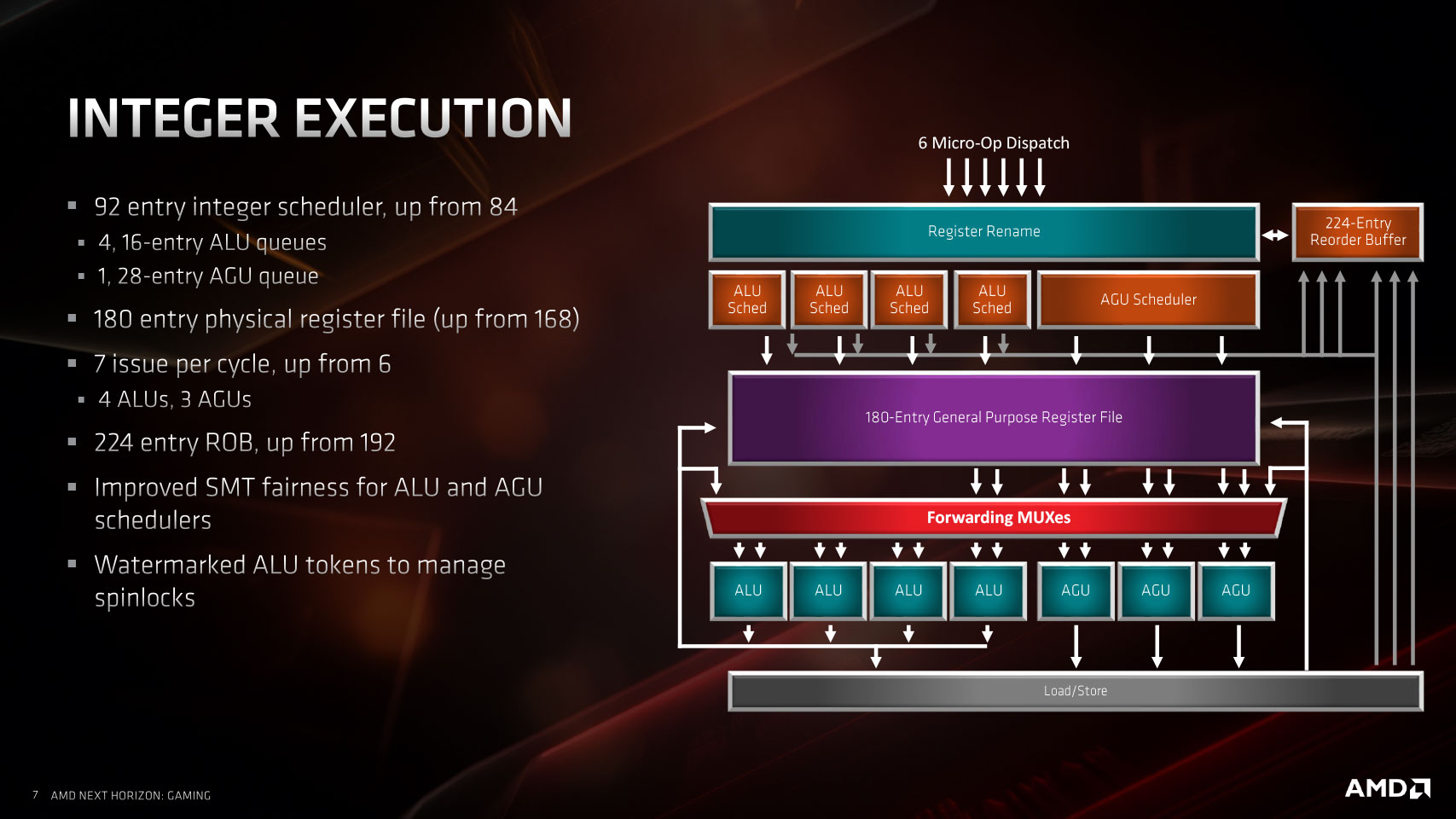
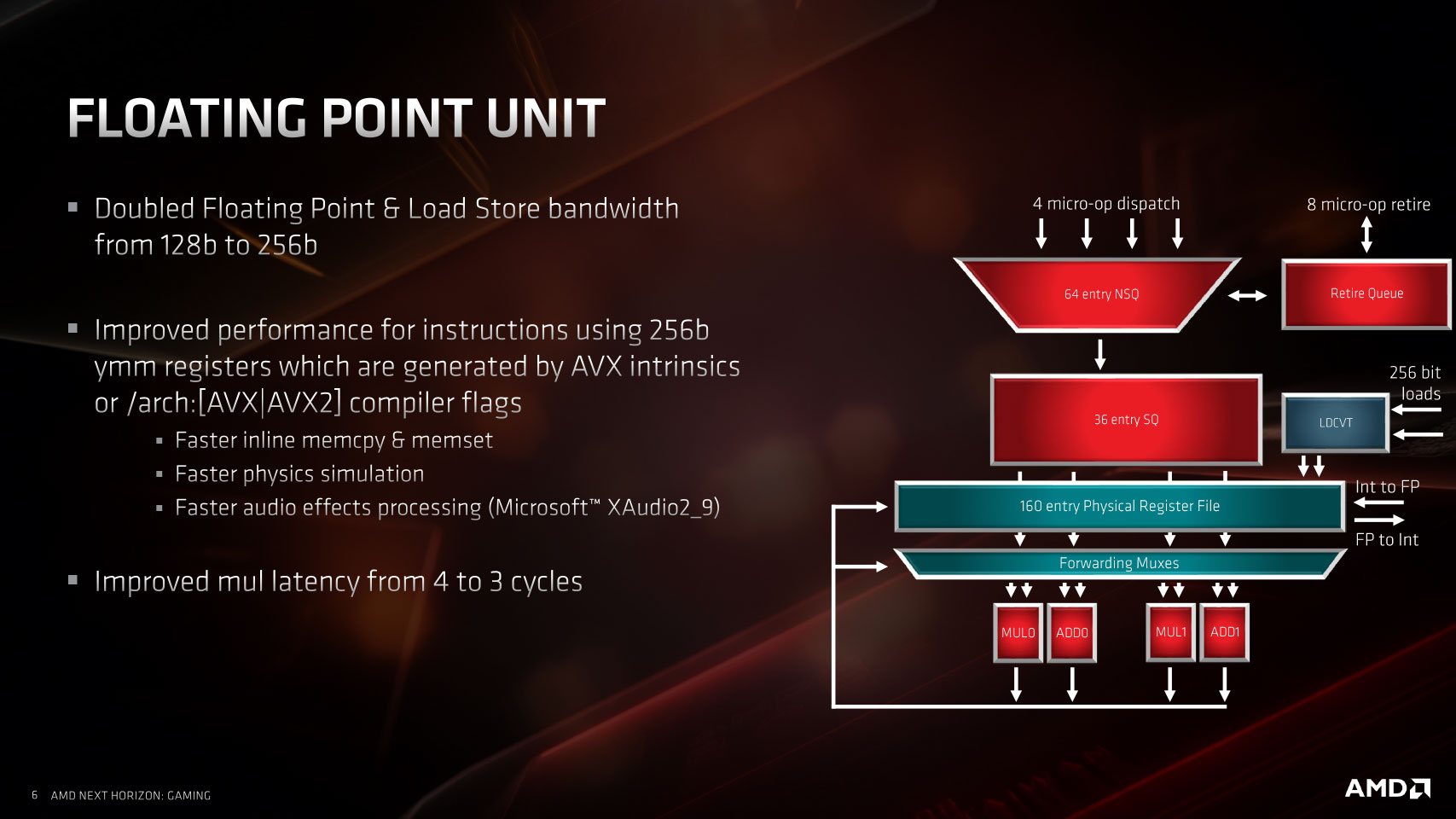
We now move on to the two components that contribute the most to the IPC, the Integer and Floating-point Units. The Integer unit receives incremental updates in the form of a broader integer scheduler that handles 92 entries (up from 84), with four 16-entry ALU queues and one 28-entry AGU queue. The general-purpose physical register file has now been expanded to 180 entries, up from 168. The issue-per-cycle has been broadened to 7 from 6, which now includes 4 ALUs and 3 AGUs. The reorder-buffer (ROB) has been broadened to 224 entries, up from 192. The SMT (simultaneous multi-threading) logic has been tweaked to better share the ALUs and AGUs among the logical processors. The FPU has the bulk of the innovation with "Zen 2". The load/store bandwidth of the FPU has been doubled to 256-bit, up from 128-bit on "Zen".
The core now also supports a sort of AVX-256: AVX/AVX2-flagged instructions with 256-bit registers. There are many applications for this, such as physics simulation, audio-stack execution, and memory-copy performance improvement. Multiplication operation latency has been improved by 33 percent.

Lastly, we move on to the Load/Store unit with a similar round of generational enhancements. The entry store queue is expanded to 48 entries, up from 44. The L2 TLB (translation lookaside buffer) has been expanded by 33% to 2,000 entries, and its latency improved. The 32 KB L1 Data cache has two 256-bit read paths and one 256-bit write path, with 64-byte load and 32-byte store alignment boundaries. The load/store bandwidth to L2 has been doubled to 32 bytes per clock.

We now move on to the cache hierarchy, which is essentially the same as "Zen." Notwithstanding the technical changes described above, the "Zen 2" core still has a 32 KB 8-way L1I cache, 32 KB 8-way L1D cache, and a dedicated 512 KB 8-way L2 cache. AMD doubled the shared L3 cache size to 16 MB. Every CCX (quad-core compute complex) on a "Zen 2" processor now has 16 MB of shared L3 cache. The doubling in L3 cache size was necessary not just because Intel shares larger amounts of L3 cache among individual cores on the "Coffee Lake Refresh" silicon (16 MB shared among all 8 cores), but also because the larger L3 cache on a "Zen 2" CCX cushions data transfers with the I/O controller die.
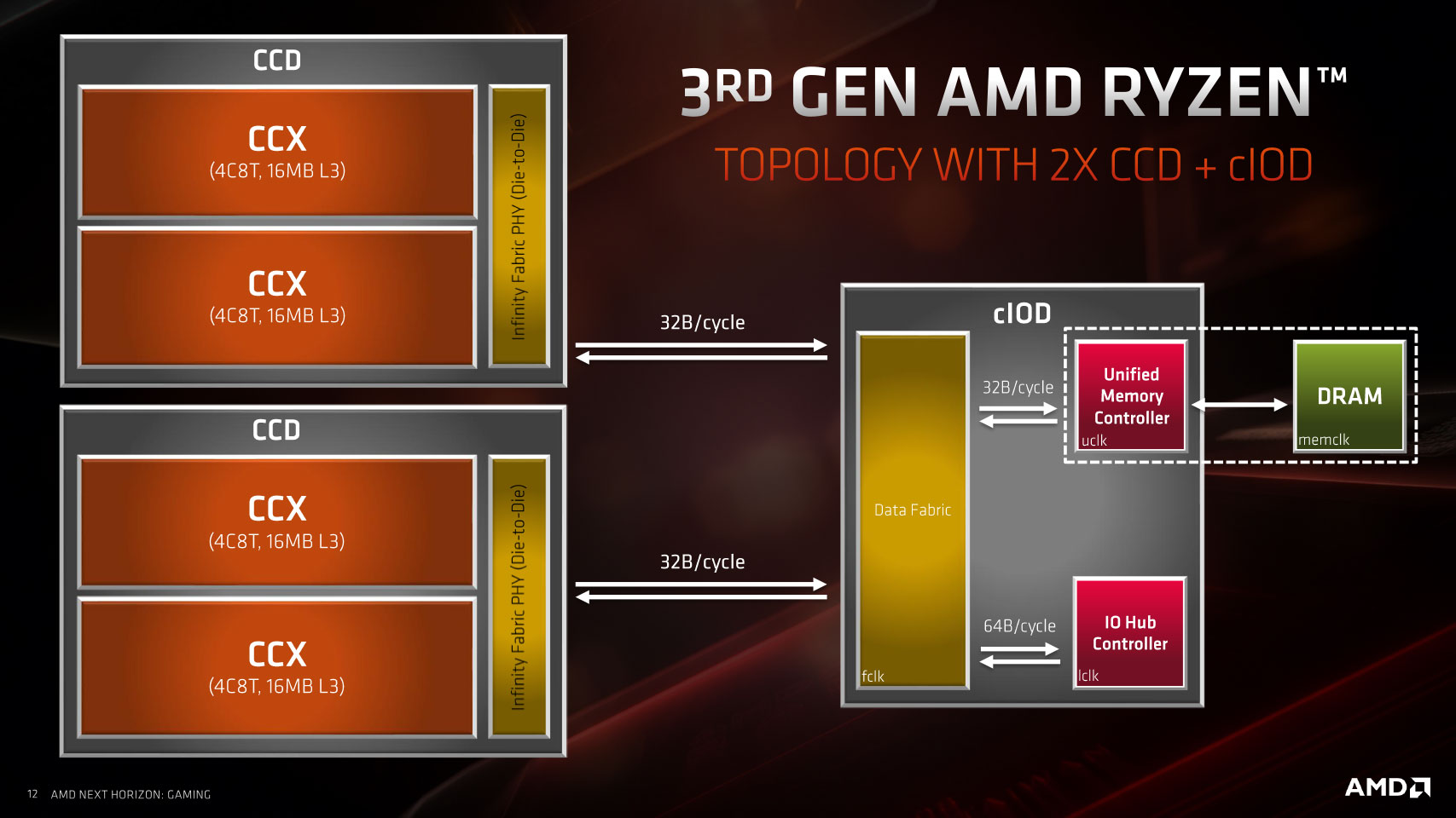
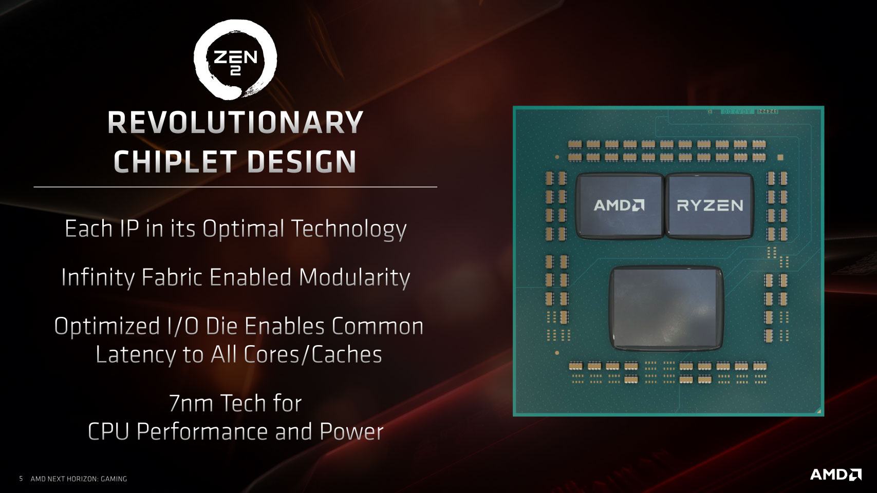
This brings us to the interesting and quirky way AMD achieved 16 cores. The Ryzen 9 3900X and Ryzen 7 3700X processor packages are codenamed "Matisse". This is a multi-chip module (MCM) of one or two 7 nm 8-core "Zen 2" CPU chiplets and one I/O controller die built on the 12 nm process. AMD made sure only those components that tangibly benefit from the shrink to 7 nm—namely, the CPU cores—are built on the new process, while those components that don't benefit from 7 nm stay on the existing 12 nm process, on the I/O controller die.

These components include the processor's dual-channel DDR4 memory controller; a 24-lane PCI-Express gen 4.0 root-complex, and an integrated southbridge that puts out some platform connectivity directly from the AM4 socket, such as SATA 6 Gbps and USB 3.1 ports. Infinity Fabric is the interconnect that binds the three dies by providing a 100 GB/s data path between each CPU chiplet and the I/O controller. The memory clock is now practically de-coupled from the Infinity Fabric clock, which should improve memory overclocking headroom. AMD also claims to have put in a lot of work to improving memory module compatibility across brands, especially since Samsung stopped mass-production of the expensive B-die DRAM chip that favored AMD processors. The memory scaling article talks a little more about this.
AMD "Valhalla" X570 Desktop Platform

AMD delivered on its promise of 3rd generation Ryzen "Matisse" processors being backwards compatible with older socket AM4 motherboards, going all the way back to the AMD 300-series chipset, with a simple BIOS update. To make the most out of Ryzen "Matisse"—namely, PCI-Express gen 4.0 connectivity and increased CPU/memory overclocking headroom, you're expected to use one of the latest motherboards that use the AMD X570 chipset. The X570 is an entirely different chip from the X470 and X370. The older chipsets were supplied by ASMedia, and were rather slim in their downstream connectivity.
The X470 only puts out 8 PCIe gen 2.0 downstream lanes, for example. The X570 modernizes all I/O by putting out up to 16 PCIe gen 4.0 downstream lanes. This enables additional M.2 PCIe gen 4 slots on your motherboards for the latest SSDs featuring PCIe gen 4 support and creates room for many new bandwidth-hungry onboard devices, such as 10 GbE adapters, next-generation Thunderbolt, 802.11ax controllers, etc. Along with the "Matisse" SoC, the X570 also puts out a number of 10 Gbps USB 3.1 gen 2 ports. Motherboards based on X570 also implement modern network connectivity options, such as 2.5 GbE and 802.11ax WLAN.
Apr 16th, 2024 12:52 EDT
change timezone
Latest GPU Drivers
New Forum Posts
- Time to update the motherboards layout! (104)
- ThrottleStop Only Applying CPU Core Offset, NOT CPU Cache Offset (22)
- Free Games Thread (3752)
- Dell Workstation Owners Club (3048)
- Outer Worlds getting boring (20)
- The TPU Darkroom - Digital SLR and Photography Club (3946)
- Some VR for Mom (7)
- DTS DCH Driver for Realtek HDA [DTS:X APO4 + DTS Interactive] (1893)
- What's your latest tech purchase? (20233)
- Cyberpunk 2077 Game Discussion (2117)
Popular Reviews
- Horizon Forbidden West Performance Benchmark Review - 30 GPUs Tested
- PowerColor Radeon RX 7900 GRE Hellhound Review
- Galax GeForce RTX 4070 Super EX Review
- Fractal Design Terra Review
- ASUS GeForce RTX 4090 Matrix Platinum Review - The RTX 4090 Ti
- Corsair 2000D Airflow Review
- Minisforum EliteMini UM780 XTX (AMD Ryzen 7 7840HS) Review
- Creative Pebble X Plus Review
- FiiO KB3 HiFi Mechanical Keyboard Review - Integrated DAC/Amp!
- ASUS GeForce RTX 4090 STRIX OC Review
Controversial News Posts
- NVIDIA Points Intel Raptor Lake CPU Users to Get Help from Intel Amid System Instability Issues (102)
- US Government Wants Nuclear Plants to Offload AI Data Center Expansion (98)
- Sony PlayStation 5 Pro Specifications Confirmed, Console Arrives Before Holidays (92)
- Developers of Outpost Infinity Siege Recommend Underclocking i9-13900K and i9-14900K for Stability on Machines with RTX 4090 (82)
- Windows 10 Security Updates to Cost $61 After 2025, $427 by 2028 (79)
- TechPowerUp Hiring: Reviewers Wanted for Motherboards, Laptops, Gaming Handhelds and Prebuilt Desktops (70)
- Intel Realizes the Only Way to Save x86 is to Democratize it, Reopens x86 IP Licensing (70)
- AMD Zen 5 Execution Engine Leaked, Features True 512-bit FPU (63)