 173
173
AMD Ryzen 9 3900X Review
(173 Comments) »Introduction
AMD today released its 3rd generation Ryzen desktop processor family based on its "Zen 2" microarchitecture. The company surprised everyone with its "Zen" desktop family because expectations from AMD on the processor front had faded due to a decade of Intel's unchallenged market dominance and its eventual stagnation in per-core performance growth over the past few years. Something as simple as a 4% IPC uplift from AMD for its 2nd generation "Zen+" processors was met with cheers as Intel began waking up to the reality of a resurgent AMD. Wafer supply woes causing price hikes shielded AMD from Intel's 8th generation Core. Intel fought back with the 9th generation Core processors, but pricing and supply issues in the desktop retail channel pushed sales to AMD. Fast forward to mid-2019 and AMD is in the thick of things.
Today, AMD is not only launching its 3rd generation Ryzen processors, but also its Radeon RX 5700 "Navi" graphics cards. What's common between the two is the 7 nanometer silicon fabrication process they're built on, which is significantly more advanced than the 14 nm process Intel has been stuck with. With Intel's upcoming 10 nm "Ice Lake" processors arriving no sooner than 2020 for the desktop platform, AMD is eyeing a free rein on the market for a good three quarters by releasing "Zen 2" with the idea of toppling Intel's 9th generation Core processors at every price point.
At the heart of AMD's effort is the "Zen 2" microarchitecture, which sets out to match or exceed the IPC of Intel's latest "Coffee Lake" microarchitecture. This would be the first time in over 15 years that AMD beats Intel at IPC. While Intel led AMD at IPC, AMD led Intel at CPU core count. Intel responded to previous generations of Ryzen processors by increasing core counts of its mainstream desktop processors for the first time in a decade. With the 9th generation Core, Intel achieved core-count parity. AMD's response is not only matching the 9th generation Core at IPC, but also restoring AMD's competitiveness by increasing core counts, at least in the high end. Intel gave its coveted Core i9 brand extension to its 8-core LGA1151 processor. AMD created the new Ryzen 9 series to match the Core i9 LGA1151 at price and IPC, while beating it at core counts. We hence have the Ryzen 9 3900X and the upcoming 3950X.
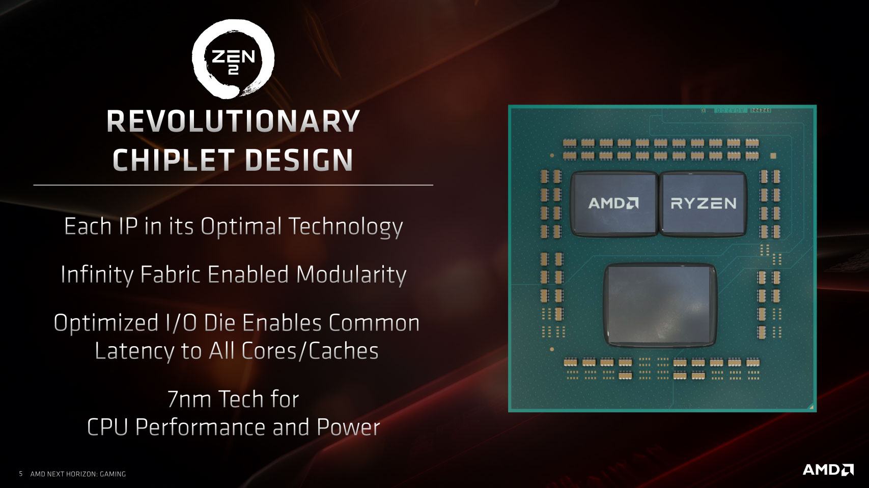
The Ryzen 9 3900X is a 12-core/24-thread processor, a 50% increase in core counts right off the bat against the Core i9-9900K. The Ryzen 9 3950X, which will join the product stack this fall, is a 16-core/32-thread monstrosity priced at $750, while retaining its mainstream-desktop credentials. Such high core counts are possibly not only due to the switch to 7 nm, but also because AMD has taken the multi-chip module (MCM) approach to building these processors, which are both similar and dissimilar to the Ryzen Threadripper. They're similar in that the CPU cores are spread across two separate dies. They're dissimilar in that there's a second kind of die, the I/O controller.
With its first EPYC and Ryzen Threadripper processors, particularly the high core-count WX models, AMD ran into several structural problems with memory bandwidth sharing between the CPU cores. The company fixed these with its 2nd generation EPYC processors in which all dies with CPU cores talk to a centralized I/O controller die that has a monolithic memory controller, thereby making it possible for a CPU core to have the full bus width of the memory interface. With its 3rd generation Ryzen processors, AMD takes a similar approach. Two 8-core CPU complex dies talk to an I/O controller die over Infinity Fabric, which has the processor's dual-channel memory interface and PCI-Express root complex.
The reasons for not building a monolithic 16-core die on 7 nm are economic. AMD is contracting TSMC to build its 7 nm wares, and it would want to minimize its silicon design to the smallest indivisible unit, an 8-core "Zen 2" chiplet. The company can build socket AM4 Ryzen processors with one or two of these chiplets to achieve up to 16 cores or drop up to eight of these on an SP3r2/TR4 package to achieve up to 64 cores. To minimize redundant components like with MCMs that use "Zeppelin" dies, AMD disintegrated the memory controller, PCIe root complex, and integrated southbridge on to the I/O controller die. This die has components that aren't as power critical as CPU cores, so AMD could build it on the existing 12LPP (12 nm) process at GlobalFoundries. The Ryzen 9 3900X is an MCM with two 7 nm CPU core chiplets, and the I/O controller die. Models that have 8 CPU cores or less, such as the Ryzen 7 3700X or the Ryzen 5 3600X, only have one 7 nm chiplet besides the I/O controller die. This way, AMD makes the most out of its limited allocation at TSMC, which is building 7 nm chips for a dozen other companies.
In this review, we have with us the Ryzen 7 3700X, an 8-core/16-thread processor launched at the same $329 price as the 2700X and over $50 cheaper than the Core i7-9700K. Besides a higher core count and similar IPC, these processors offer the latest PCI-Express gen 4.0 bus, which doubles bandwidth for graphics cards and SSDs that support it.
Our exhaustive coverage of AMD's 7/7 Launch Day includes the following content:
AMD Ryzen 9 3900X 12-core processor | AMD Ryzen 7 3700X 8-core processor | AMD Radeon RX 5700 XT graphics card | AMD Radeon RX 5700 graphics card | AMD Zen 2 Memory Performance Scaling | Ryzen 3900X and 3700 on X470 vs X570 platforms | Radeon RX 5700 XT Navi PCI-Express 4.0 Performance Scaling | ASRock X570 Taichi motherboard | ASUS Prime X570-Pro motherboard
| Price | Cores / Threads | Base Clock | Max. Boost | L3 Cache | TDP | Architecture | Process | Socket | |
|---|---|---|---|---|---|---|---|---|---|
| Core i7-9600K | $230 | 6 / 6 | 3.7 GHz | 4.6 GHz | 9 MB | 95 W | Coffee Lake | 14 nm | LGA 1151 |
| Ryzen 5 2600X | $170 | 6 / 12 | 3.6 GHz | 4.2 GHz | 16 MB | 95 W | Zen | 12 nm | AM4 |
| Ryzen 7 1700X | $170 | 8 / 16 | 3.4 GHz | 3.8 GHz | 16 MB | 95 W | Zen | 14 nm | AM4 |
| Ryzen 7 2700 | $235 | 8 / 16 | 3.2 GHz | 4.1 GHz | 16 MB | 65 W | Zen | 12 nm | AM4 |
| Core i7-8700K | $365 | 6 / 12 | 3.7 GHz | 4.7 GHz | 12 MB | 95 W | Coffee Lake | 14 nm | LGA 1151 |
| Core i7-9700K | $410 | 8 / 8 | 3.6 GHz | 4.9 GHz | 12 MB | 95 W | Coffee Lake | 14 nm | LGA 1151 |
| Ryzen 7 2700X | $295 | 8 / 16 | 3.7 GHz | 4.3 GHz | 16 MB | 105 W | Zen | 12 nm | AM4 |
| Ryzen 7 1800X | $250 | 8 / 16 | 3.6 GHz | 4.0 GHz | 16 MB | 95 W | Zen | 14 nm | AM4 |
| Ryzen 7 3700X | $330 | 8 / 16 | 3.6 GHz | 4.4 GHz | 32 MB | 65 W | Zen 2 | 7 nm | AM4 |
| Core i9-9900K | $480 | 8 / 16 | 3.6 GHz | 5.0 GHz | 16 MB | 95 W | Coffee Lake | 14 nm | LGA 1151 |
| Ryzen 9 3900X | $500 | 12 / 24 | 3.8 GHz | 4.6 GHz | 64 MB | 105 W | Zen 2 | 7 nm | AM4 |
| Threadripper 2920X | $635 | 12 / 24 | 3.5 GHz | 4.3 GHz | 32 MB | 180 W | Zen | 12 nm | SP3r2 |
| Threadripper 2950X | $830 | 16 / 32 | 3.5 GHz | 4.4 GHz | 32 MB | 180 W | Zen | 12 nm | SP3r2 |
A Closer Look
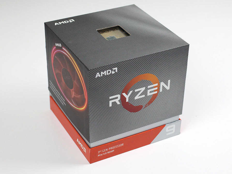
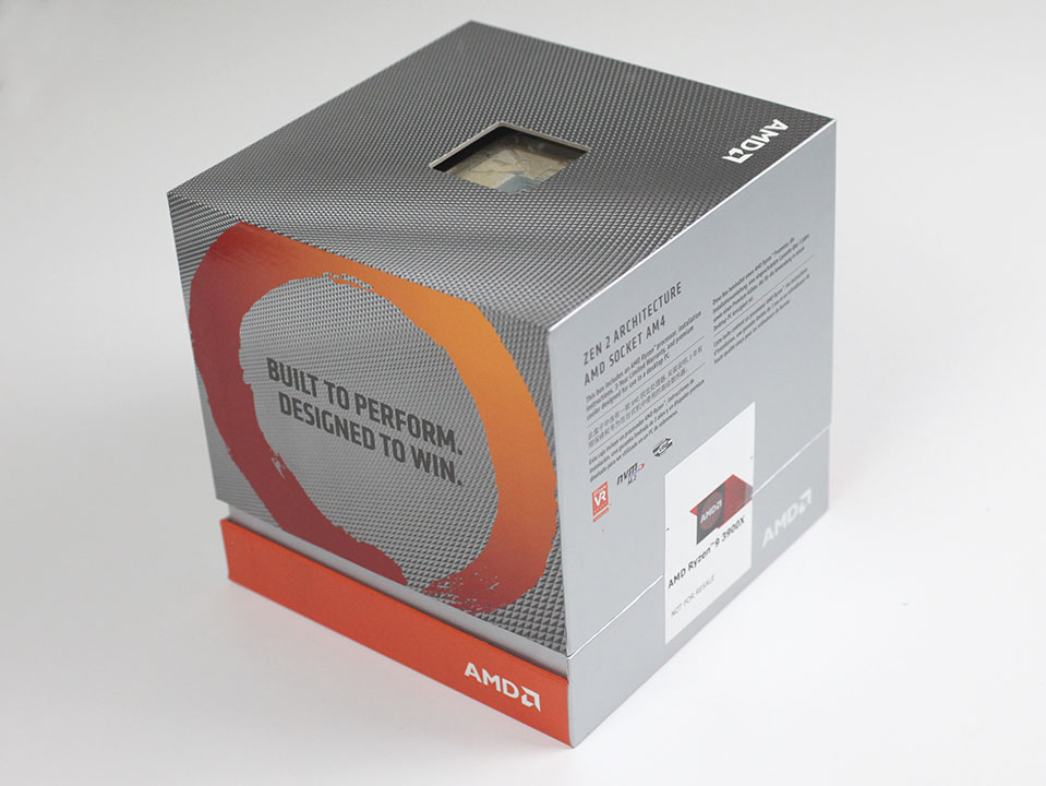
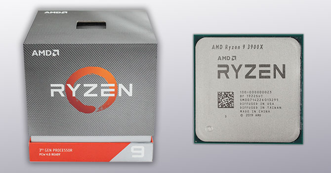
The Ryzen 9 3900X ships in a large cubical paperboard box with carbon-fiber texture on some of its faces. This box looks more premium than the one the Ryzen 7 ships in and has a clam-shell design. There are clear markings on the front that tell you that this is a 3rd generation Ryzen processor, which has PCI-Express gen 4.0 support. The back also mentions "Zen 2". There are also some "VR ready" and NVMe logos on the box.
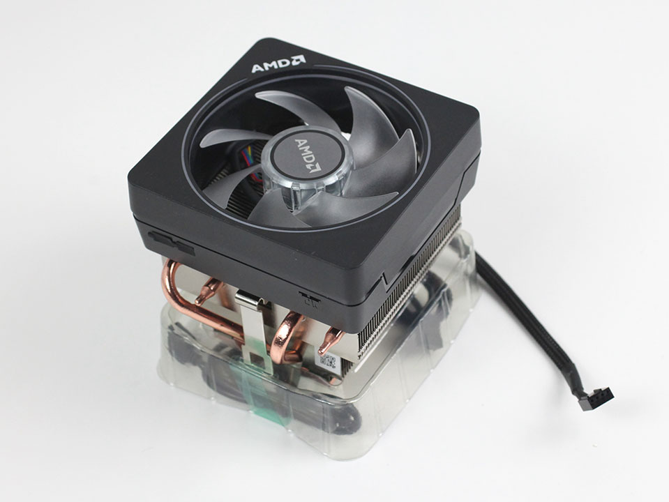
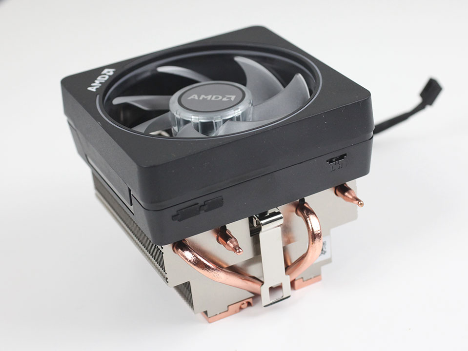
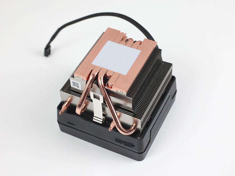
AMD includes a Wraith Prism RGB cooling solution with this processor capable of thermal loads of up to 140 W.

Besides 4-pin PWM for its fan, the cooler includes two additional cables, an addressable 3-pin RGB cable to control the lighting and a USB cable that plugs into one of your motherboard's USB 2.0/1.1 headers. Both cables are optional. You only need to plug in the 4-pin PWM connector for the fan to spin.
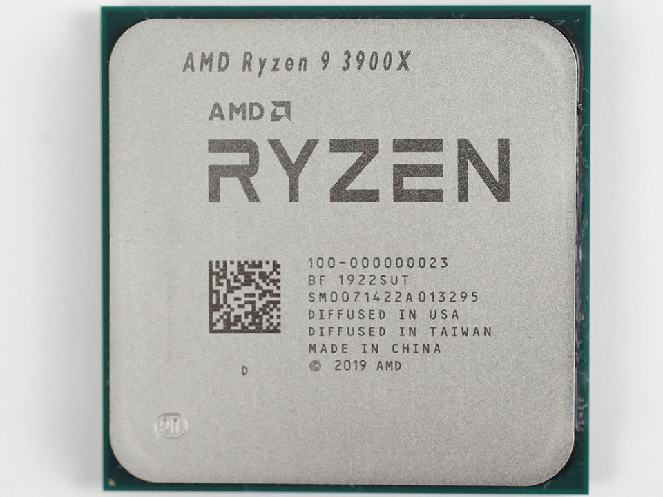
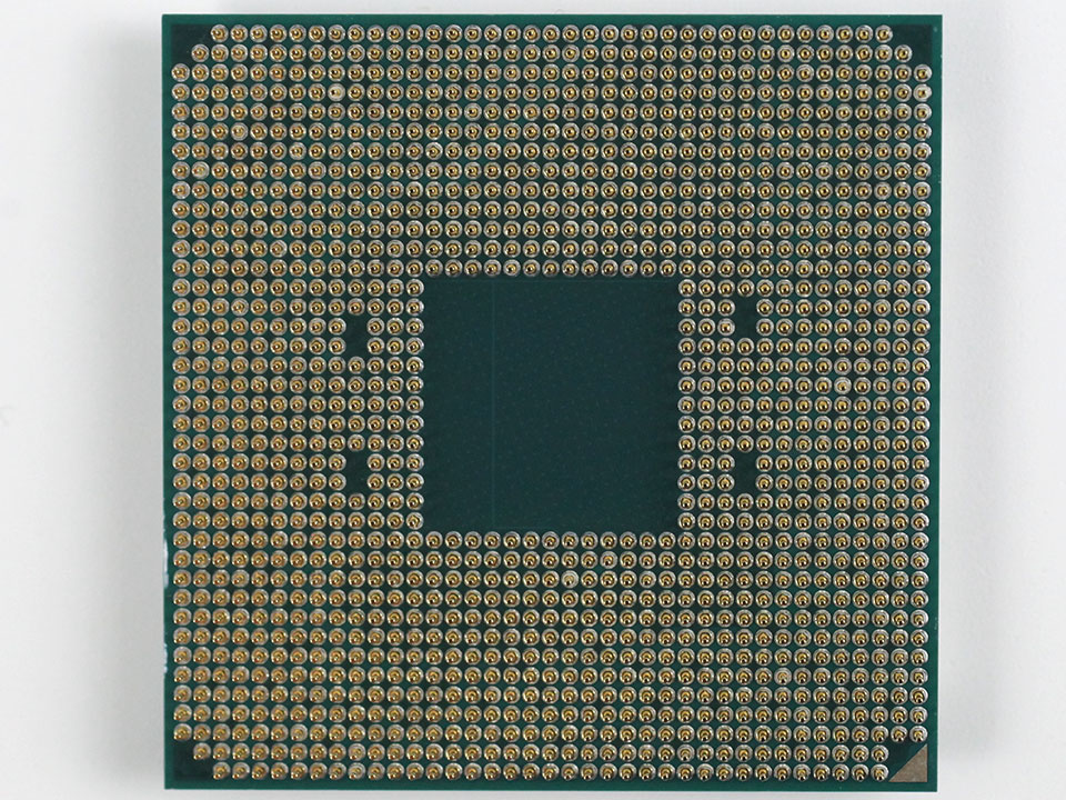
The Ryzen 9 3900X processor looks like any other conventional AMD processor, with a large IHS dominating the top and a 1,331-pin micro-PGA in the bottom. You see national-origin markings for three places—USA, China, and Taiwan. The 7 nm "Zen 2" CPU chiplets are made in TSMC, Taiwan. The 12 nm I/O controller die is made in the US at GlobalFoundries. The two dies are packaged into the MCM at a facility in China.
Architecture
AMD's 3rd generation Ryzen processors use the "Zen 2" microarchitecture. The 2nd generation Ryzen chips use an enhanced first-generation "Zen" derivative called "Zen+", which has process and boost algorithm improvements eke out roughly a 4% IPC uplift. With "Zen 2", AMD's key design goal is to finally beat Intel in the IPC game. IPC, or instructions per clock, is loosely used to denote a CPU core's performance at a given clock speed. For the past 15 or so years, Intel dominated AMD at IPC, while AMD attempted to make their processors competitive by cramming in more CPU cores than Intel at any given price point for competitive multi-threaded performance. Today's software environment is increasingly multi-threaded, as are games. With "Zen 2", AMD set itself an ambitious double-digit-percentage IPC uplift target to catch up or overtake Intel's latest "Coffee Lake" microarchitecture at IPC. AMD didn't stop there and even increased core counts for the platform at higher price points. The 3rd generation Ryzen family even includes a 16-core processor, which is a tremendous core count for the mainstream-desktop platform.


Before we get into the interesting and quirky way AMD crammed 16 cores into this chip, let's talk about the "Zen 2" CPU core. After the colossal failure that was "Bulldozer," AMD set out to once again build strong and monolithic CPU cores that share nothing except L3 cache with other cores. It achieved this desired result with "Zen", which posted a mammoth 40%–50% IPC increase over "Bulldozer", catapulting AMD back into competitiveness. "Zen" cores IPC sits somewhere between "Haswell" and "Skylake/Coffee Lake", which was enough for AMD as it backed the IPC increase with higher core counts compared to Intel. Over the 8th and 9th generations of Core processors that retained the same IPC as "Skylake", Intel shored up core counts to match AMD. Wanting to set up a definitive edge over Intel, AMD not only worked to increase IPC, but also core counts.
The "Zen 2" CPU core has essentially the same component layout and hierarchy as "Zen", but with major changes and broadening of key components. As with "Zen" (or most x86 CPU cores), the "Zen 2" core is made up of five key components: Fetch, Decode, Integer, Floating-point, and load-store. Fetch and Decode tell the CPU core what needs to be done and what data or instructions are needed; Integer and Floating-Point Unit execute a mathematical model of what needs to be done depending on the data type and nature of the instruction; Load/Store are the I/O of the CPU core. At various levels, there are tiny buffers, registers that store instructions, and larger caches that cushion data-transfers between various components.


AMD updated the Fetch and Decode units, which contribute to IPC, by making the CPU work "smarter". The updated Integer and FPU make the CPU work "harder", the Load/Store unit's job is to make sure the other components aren't starved of things to do. The Fetch unit is updated with a TAGE branch predictor. Invented in 2006, TAGE is considered to be the best branch-prediction technique by the IEEE. AMD broadened the BTB (branch target buffers) at L1 and L2 by doubling the L1 entries to 512k, and L2 entries to 7,000 from 4,000. The ITA (indirect target array) has also been expanded. The design goal for updating the Fetch unit is to lower "mispredictions" (bad guesses) that wasted load/storage operations by 30 percent. The 32 KB L1 instruction cache has also been improved. The Decode unit has two improvements to the Op cache: improved instruction fusion and the ability to push up to 4,000 fused instructions per clock cycle.
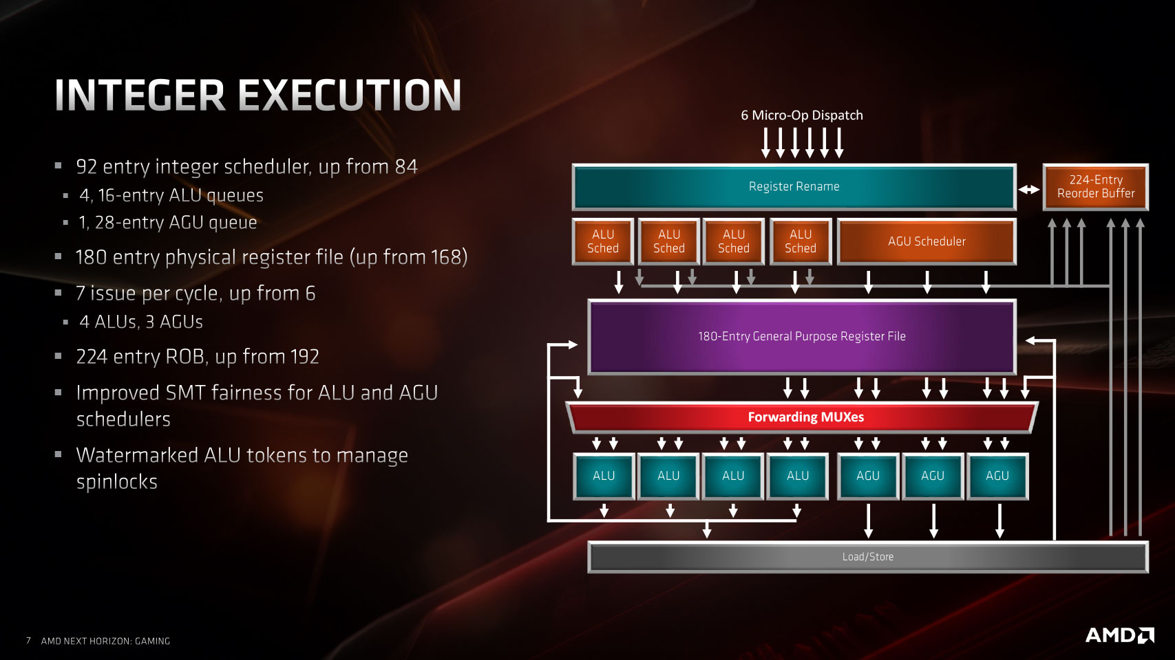
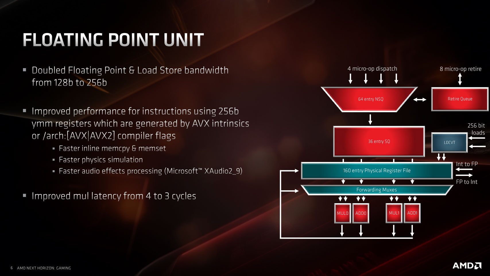
We now move on to the two components that contribute the most to the IPC, the Integer and Floating-point Units. The Integer unit receives incremental updates in the form of a broader integer scheduler that handles 92 entries (up from 84), with four 16-entry ALU queues and one 28-entry AGU queue. The general-purpose physical register file has now been expanded to 180 entries, up from 168. The issue-per-cycle has been broadened to 7 from 6, which now includes 4 ALUs and 3 AGUs. The reorder-buffer (ROB) has been broadened to 224 entries, up from 192. The SMT (simultaneous multi-threading) logic has been tweaked to better share the ALUs and AGUs among the logical processors. The FPU has the bulk of the innovation with "Zen 2". The load/store bandwidth of the FPU has been doubled to 256-bit, up from 128-bit on "Zen".
The core now also supports a sort of AVX-256: AVX/AVX2-flagged instructions with 256-bit registers. There are many applications for this, such as physics simulation, audio-stack execution, and memory-copy performance improvement. Multiplication operation latency has been improved by 33 percent.

Lastly, we move on to the Load/Store unit with a similar round of generational enhancements. The entry store queue is expanded to 48 entries, up from 44. The L2 TLB (translation lookaside buffer) has been expanded by 33% to 2,000 entries, and its latency improved. The 32 KB L1 Data cache has two 256-bit read paths and one 256-bit write path, with 64-byte load and 32-byte store alignment boundaries. The load/store bandwidth to L2 has been doubled to 32 bytes per clock.

We now move on to the cache hierarchy, which is essentially the same as "Zen." Notwithstanding the technical changes described above, the "Zen 2" core still has a 32 KB 8-way L1I cache, 32 KB 8-way L1D cache, and a dedicated 512 KB 8-way L2 cache. AMD doubled the shared L3 cache size to 16 MB. Every CCX (quad-core compute complex) on a "Zen 2" processor now has 16 MB of shared L3 cache. The doubling in L3 cache size was necessary not just because Intel shares larger amounts of L3 cache among individual cores on the "Coffee Lake Refresh" silicon (16 MB shared among all 8 cores), but also because the larger L3 cache on a "Zen 2" CCX cushions data transfers with the I/O controller die.
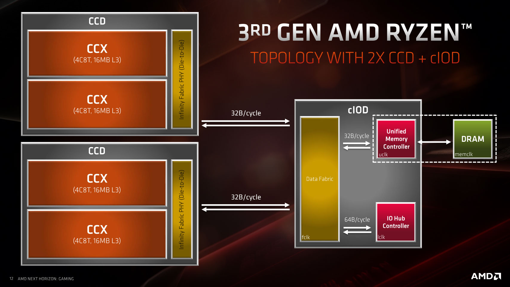
This brings us to the interesting and quirky way AMD achieved 16 cores. The Ryzen 9 3900X and Ryzen 7 3700X processor packages are codenamed "Matisse". This is a multi-chip module (MCM) of one or two 7 nm 8-core "Zen 2" CPU chiplets and one I/O controller die built on the 12 nm process. AMD made sure only those components that tangibly benefit from the shrink to 7 nm—namely, the CPU cores—are built on the new process, while those components that don't benefit from 7 nm stay on the existing 12 nm process, on the I/O controller die.

These components include the processor's dual-channel DDR4 memory controller; a 24-lane PCI-Express gen 4.0 root-complex, and an integrated southbridge that puts out some platform connectivity directly from the AM4 socket, such as SATA 6 Gbps and USB 3.1 ports. Infinity Fabric is the interconnect that binds the three dies by providing a 100 GB/s data path between each CPU chiplet and the I/O controller. The memory clock is now practically de-coupled from the Infinity Fabric clock, which should improve memory overclocking headroom. AMD also claims to have put in a lot of work to improving memory module compatibility across brands, especially since Samsung stopped mass-production of the expensive B-die DRAM chip that favored AMD processors. The memory scaling article talks a little more about this.
AMD "Valhalla" X570 Desktop Platform

AMD delivered on its promise of 3rd generation Ryzen "Matisse" processors being backwards compatible with older socket AM4 motherboards, going all the way back to the AMD 300-series chipset, with a simple BIOS update. To make the most out of Ryzen "Matisse"—namely, PCI-Express gen 4.0 connectivity and increased CPU/memory overclocking headroom, you're expected to use one of the latest motherboards that use the AMD X570 chipset. The X570 is an entirely different chip from the X470 and X370. The older chipsets were supplied by ASMedia, and were rather slim in their downstream connectivity.
The X470 only puts out 8 PCIe gen 2.0 downstream lanes, for example. The X570 modernizes all I/O by putting out up to 16 PCIe gen 4.0 downstream lanes. This enables additional M.2 PCIe gen 4 slots on your motherboards for the latest SSDs featuring PCIe gen 4 support and creates room for many new bandwidth-hungry onboard devices, such as 10 GbE adapters, next-generation Thunderbolt, 802.11ax controllers, etc. Along with the "Matisse" SoC, the X570 also puts out a number of 10 Gbps USB 3.1 gen 2 ports. Motherboards based on X570 also implement modern network connectivity options, such as 2.5 GbE and 802.11ax WLAN.
Test Setup
| Test System "Zen 2" | |
|---|---|
| Processor: | All AMD Ryzen 3000 |
| Motherboard: | ASRock X570 Taichi AMD X570, BIOS v1.30 |
| Memory: | 2x 8 GB G.SKILL Flare X DDR4 DDR4-3200 14-14-14-34 |
| Graphics: | EVGA GeForce RTX 2080 Ti FTW3 Ultra |
| Storage: | 1 TB SSD |
| Power Supply: | Seasonic SS-860XP |
| Software: | Windows 10 Professional 64-bit Version 1903 (May 2019 Update) |
| Drivers: | NVIDIA GeForce 430.63 WHQL AMD Chipset 1.07.07.0725 |
| Test System "Zen" | |
|---|---|
| Processor: | All AMD Ryzen 2000, Ryzen 2000G and Ryzen 1000 |
| Motherboard: | MSI X470 Gaming M7 AC AMD X470, BIOS 7B77v19O |
| Memory: | 2x 8 GB G.SKILL Flare X DDR4 DDR4-3200 14-14-14-34 |
| Graphics: | EVGA GeForce RTX 2080 Ti FTW3 Ultra |
| Storage: | 1 TB SSD |
| Power Supply: | Seasonic SS-860XP |
| Software: | Windows 10 Professional 64-bit Version 1903 (May 2019 Update) |
| Drivers: | NVIDIA GeForce 430.63 WHQL AMD Chipset 1.07.07.0725 |
| Test System "Coffee Lake" | |
|---|---|
| Processor: | All Intel 8th & 9th Generation processors |
| Motherboard: | ASUS Z390 Maximus XI Extreme Intel Z390, BIOS 1105 |
| Memory: | 2x 8 GB G.SKILL Flare X DDR4 DDR4-3200 14-14-14-34 |
| Graphics: | EVGA GeForce RTX 2080 Ti FTW3 Ultra |
| Storage: | 1 TB SSD |
| Power Supply: | Seasonic SS-860XP |
| Software: | Windows 10 Professional 64-bit Version 1903 (May 2019 Update) |
| Drivers: | NVIDIA GeForce 430.63 WHQL |
- All applications, games and processors are tested with the drivers and hardware listed above—no performance results were recycled between test systems.
- All games and applications are tested using the same game version.
- All games are set to their highest quality setting unless indicated otherwise.
Our Patreon Silver Supporters can read articles in single-page format.
Apr 23rd, 2024 22:07 EDT
change timezone
Latest GPU Drivers
New Forum Posts
- CPB Enabled Boot Loop (10)
- Upgrade Build (106)
- Official Board Game Discussion (9)
- TPU's Nostalgic Hardware Club (18461)
- The TPU UK Clubhouse (24771)
- Sexy Mechanical Keyboard Thread (485)
- Realtek Modded Audio Driver for Windows 10/11 - Only for HDAUDIO (5688)
- What's your latest tech purchase? (20319)
- Post your Cinebench 2024 score (449)
- need help with motherboard/ ram compability certainty (14)
Popular Reviews
- Fractal Design Terra Review
- Corsair 2000D Airflow Review
- Thermalright Phantom Spirit 120 EVO Review
- Minisforum EliteMini UM780 XTX (AMD Ryzen 7 7840HS) Review
- ASUS GeForce RTX 4090 STRIX OC Review
- NVIDIA GeForce RTX 4090 Founders Edition Review - Impressive Performance
- ASUS GeForce RTX 4090 Matrix Platinum Review - The RTX 4090 Ti
- MSI GeForce RTX 4090 Suprim X Review
- MSI GeForce RTX 4090 Gaming X Trio Review
- Gigabyte GeForce RTX 4090 Gaming OC Review
Controversial News Posts
- Sony PlayStation 5 Pro Specifications Confirmed, Console Arrives Before Holidays (116)
- NVIDIA Points Intel Raptor Lake CPU Users to Get Help from Intel Amid System Instability Issues (106)
- AMD "Strix Halo" Zen 5 Mobile Processor Pictured: Chiplet-based, Uses 256-bit LPDDR5X (101)
- US Government Wants Nuclear Plants to Offload AI Data Center Expansion (98)
- Windows 10 Security Updates to Cost $61 After 2025, $427 by 2028 (84)
- Developers of Outpost Infinity Siege Recommend Underclocking i9-13900K and i9-14900K for Stability on Machines with RTX 4090 (84)
- TechPowerUp Hiring: Reviewers Wanted for Motherboards, Laptops, Gaming Handhelds and Prebuilt Desktops (74)
- Intel Realizes the Only Way to Save x86 is to Democratize it, Reopens x86 IP Licensing (70)